1.1mil=0.001inch=0.0254mm

oz mass unit, refers to copper thickness
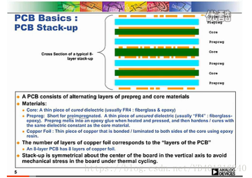
2. Layered structure
1. Trace length, width and thickness affect parasitic capacitance and inductance
2. The power supply layer and the ground layer are relatively thick: a. Shield radiation interference, crosstalk b. Reduce impedance 3.
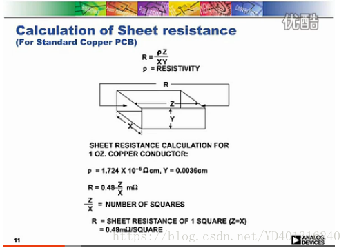
3. Trace resistance