After analyzing the principle of the entire circuit, you can start to layout and route the entire circuit. In this issue, I will introduce the ideas and principles of layout to you. 1. First of all, we will place the devices with structural requirements. When placing them, according to the imported structure, the connector must pay attention to the placement of pin 1.
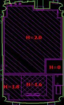
2. Pay attention to the height limit requirements in the structure when laying out.
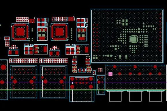
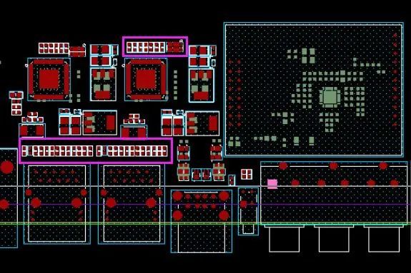
3. If you want a beautiful layout, generally locate according to the coordinates of the outer frame or center line of the component (center alignment).
4. The overall layout should consider heat dissipation.

5. When laying out, it is necessary to consider the evaluation of the wiring channel and the space required for equal length.
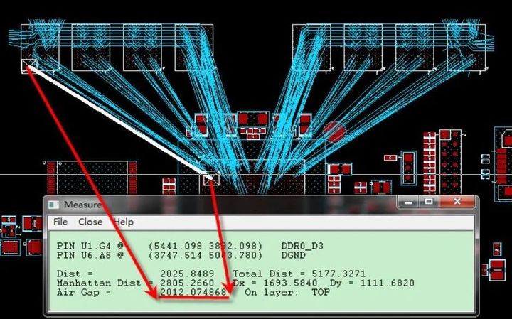
6. When laying out, it is necessary to consider the power flow direction and evaluate the power channel.
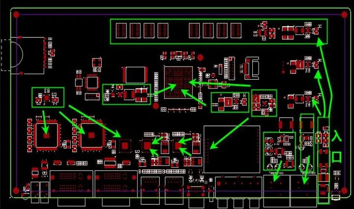
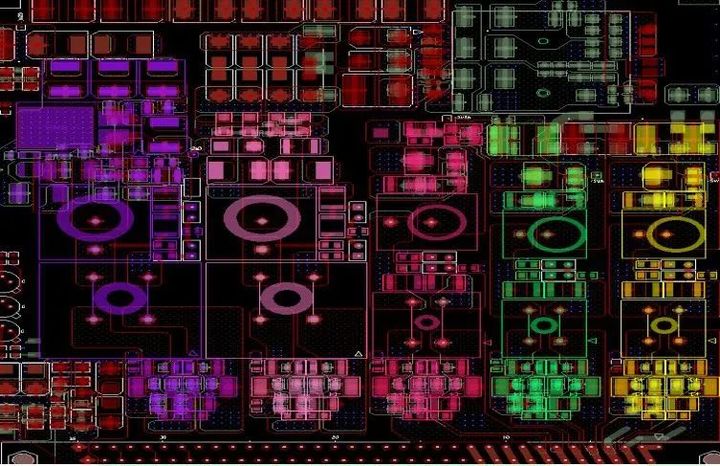
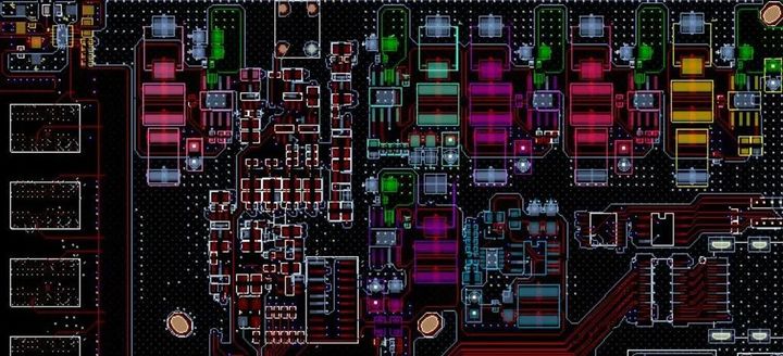
7. The high-speed, medium-speed and low-speed circuits should be separated.

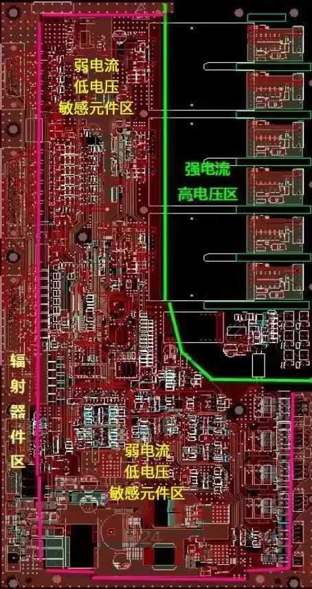
8. Keep strong current, high voltage, and strong radiation components away from weak current, low voltage, and sensitive components.
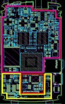
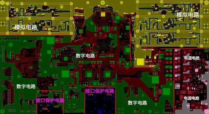
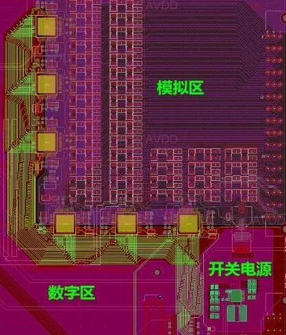
9. The analog, digital, power supply and protection circuits should be separated.
10. The interface protection device should be placed as close to the interface as possible.
11. Requirements for the placement sequence of interface protection devices:
(1) The order of general power supply lightning protection devices is: varistor, fuse, suppression diode, EMI filter, inductor or common mode inductor, and the layout of any device above is delayed if the schematic diagram is missing;
(2) Generally, the order of protection devices for interface signals is: ESD (TVS tube), isolation transformer, common mode inductor, capacitor, and resistor. For the lack of schematic diagram, any device above is sequentially laid out; strictly follow the sequence of the schematic diagram (there must be The ability to judge whether the schematic diagram is correct) for "one-line" layout.

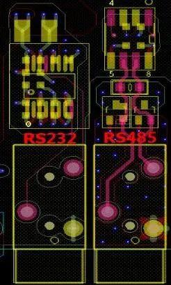
12. The level conversion chip (such as RS232) is placed close to the connector (such as serial port).
13. Devices that are susceptible to ESD interference, such as NMOS and CMOS devices, should be kept away from areas that are susceptible to ESD interference (such as the edge area of a single board).

14. Clock device layout:
(1) Crystals, crystal oscillators and clock distributors should be as close as possible to related IC devices;
(2) The filter of the clock circuit (try to use "∏" type filter) should be close to the power input pin of the clock circuit;
(3) Whether the output of the crystal oscillator and the clock distributor is connected in series with a 22-ohm resistor;
(4) Whether the unused output pin of the clock distributor is grounded through a resistor;
(5) The layout of crystals, crystal oscillators and clock distributors should be kept away from high-power components, radiators and other heat-generating devices;
(6) Whether the distance between the crystal oscillator and the interface device is greater than 1inch.

15. Whether the switching power supply is far away from AD\DA converters, analog devices, sensitive devices, and clock devices.
16. The layout of the switching power supply should be compact, and the input and output should be separated. The layout should be strictly in accordance with the requirements of the schematic diagram, and the capacitors of the switching power supply should not be placed randomly.
17. Capacitors and filter devices:
(1) The capacitor must be placed close to the power pin, and the capacitor with the smaller capacitance should be closer to the power pin;
(2) The EMI filter should be close to the input port of the chip power supply;
(3) In principle, each power supply pin has a small capacitor of 0.1uf, and an integrated circuit has one or more large capacitors of 10uf, which can be increased or decreased according to specific conditions;

—END—
Original text: Analysis of PCB layout ideas makes your layout simple from now on!
Questions about RFASK
RF Questions is a technical question-and-answer learning platform upgraded on the basis of the "Microwave RF Network" series of original technology columns. It mainly focuses on RF chips, microwave circuits, antennas, radars, satellites and other related technical fields. , antennas, radar and other industries, providing high-quality, original technical questions and answers, column articles, RF courses and other learning content. For more information, please visit: RFASK RF Questions - RF Technology R&D Service Platform | Technical Questions and Answers, Column Articles, RF Courses