[Sum] PCB layout and wiring impedance difference (rpm)
A, PCB routing differential operation
See: Altium Designer - carefully summary
PCB differential wiring already said very clearly, this does not describe.
Second, the advantages and disadvantages of differential wirings
See also: practical application in the analysis and differential signal lines LAYOUT
See: Differential Signaling - Wikipedia
(1) the difference signal
First, look at what is a differential signal it.
1, the difference signal
Differential transmission technique for signal transmission, a signal line different from the traditional practice of a ground wire, two differential transmission lines that are in the transmission signal, the two signals of the same amplitude, opposite phase. In these two signal transmission line is the differential signal. Comparing the difference signal receiving end to determine the two voltages sending end is a logical 0 or a logical 1. In the circuit board, the differential traces must be of equal length, width, in close proximity, and two lines at the same level.
General types: USB, Ethernet, PCIE, SATA, RS485, RS422, HDMI, LVDS
Used to have: +/- PM / PN TXN / TXP
2, a single-ended differential signal line go Comparative
Conventional differential signal and one signal line and one ground wire (i.e., single-ended signal) go practice lines as compared to their advantages and disadvantages are:
advantages:
anti-interference ability. Interference noise generally equivalent, and are loaded into the two signal wires, and the difference is zero, i.e., the noise does not affect the logical sense signal.
Can effectively suppress electromagnetic interference (EMI). Since two lines close proximity and equal amplitude signal, the amplitude of which two electromagnetic field coupling between the line and the ground are equal, while their opposite signal polarity, which field will cancel each other out. So on the outside electromagnetic interference is also small.
The timing accurate positioning. Receiving the differential signal is the difference between the signal amplitude of the two positive-negative line transition point is determined as a logical jump point 0/1. Ordinary single-ended signal to a threshold voltage trip point signal logic as 0/1, greater than the threshold voltage is affected by the magnitude of the voltage signal, it is not suitable for low amplitude signals.
Disadvantage:
If the area of the circuit board is very tight, single-ended signal may be one signal line, and grounding the ground plane, while the other two differential signal must go length, width, in close proximity, and the line at the same level. This often happens in the pin pitch of the chip is so small that only one pass through the case where the traces.
(So, the differential signal wirings priority)
(2) five common misconceptions about the difference
Misunderstanding: a differential signal that does not require a ground plane return path, or that the differential traces provide reflux way to each other. The reason for this misunderstanding is to confuse superficial or deep enough understanding of the mechanism of high-speed signal transmission. Although the differential circuit and the other for a similar bomb noise signals that may be present on the power and ground planes are insensitive. Partial reflux offset does not represent the ground plane to the reference plane is not a differential circuit as the signal return path, in fact, the signal return analysis, differential traces ordinary single-ended line walking mechanism is consistent, i.e., a high-frequency signal is always along refluxed minimum loop inductance, the biggest difference is that in addition to the differential line than the coupling to ground, there is also mutual coupling, which strongly coupled, that kind of becomes the main return passage.
In the PCB circuit design, between the differential traces generally smaller coupling, often only 10 to 20% coupling, coupling more or ground, so the main return path for the differential traces still present in the ground plane . Discontinuity occurs when the local plane, without reference plane areas, provide the primary return path difference between the lines will be coupled down. Although the reference plane discontinuities influence on the differential traces of no ordinary single-ended traces to the grave, but still can degrade the quality of the differential signal, increasing the EMI, should be avoided. Some designs also believe that the difference can be removed down to the reference plane beneath the line section to suppress common mode signals in the differential transmission, but this approach is not desirable in theory, how to control the impedance? Do not give common-mode signal impedance to ground loops, is bound to cause EMI radiation, this approach is more harm than good.
Therefore, to keep the PCB ground plane return path wide and short. Try not to inter-island (or power across adjacent partition formation region). For example, the design of the motherboard USB and SATA and PCI-EXPRESS and so best not to have inter-island approach. The following signals are to ensure complete ground or power plane.
Myth: that is more important than maintaining equidistance line length matching. In actual PCB wiring, often can not meet the requirement of differential design. Because of the distribution of pins, vias, and traces space and other factors, must achieve long line winding through appropriate matching of talent, but the result must be brought part of the region can not be a differential pair in parallel, in fact, caused by unequal spacing the impact is minimal, comparatively speaking, does not match the line length is much greater influence on the timing. And from the theoretical analysis, although it will result in inconsistent spacing differential impedance changes, but because of the coupling between the differential itself is not significant, the impedance variation range is very small, typically less than 10%, the equivalent of only a via reflection caused by this signal will not cause significant influence. Once the line length does not match, in addition to the timing offset occurs, the introduction of a differential signal component back to common mode, reducing the quality of the signal, increasing the EMI.
It can be said that the differential traces of PCB design is the most important rule is to match the line length, other rules can be flexibly depending on design requirements and practical application. Meanwhile, in order to compensate for a matching impedance matching resistor may be added between the receiving terminal of the differential pair employed. Its value should be equal to the value of the differential impedance. Such signal quality would be better.
It is recommended that the following two points:
(A) using a terminal resistor maximum matching of differential transmission lines, the resistance is generally between 90 ~ 130Ω, this system also requires the terminal resistors to produce a differential voltage of normal operation;
(B) preferably used 1 to 2% of a surface mount resistor is connected across the accuracy of the differential line, if necessary, may also be used for the two respective resistors the resistance of 50Ω, and an intermediate earth via a capacitor to filter out common mode noise.
Typically for a differential signal CLOCK and other requirements of the long match the requirements within +/- 10mils.
Myth: that the differential traces must rely on the close. Let differential traces close to nothing more than to enhance their coupling, can enhance immunity to noise, but also take full advantage of the magnetic field of opposite polarity to offset the electromagnetic interference from the outside world. Although in most cases this approach is very beneficial, but not absolute, if we can ensure that they are adequately shielded from external interference, then we would not need to let through a strongly coupled to each other to achieve immunity the purpose of the suppression and EMI. How can we ensure that the differential traces with good isolation and shielding it? Increasing the pitch of other signal traces is the most basic way, electromagnetic field energy is decreasing as the distance form the square, generally more than 4 times the line width of the line spacing, interference between them on the very weak, basic can be omitted. Further, by isolating the ground plane may also play a very good shielding effect, this configuration is often used in a high frequency IC package using PCB design (10G above), known as CPW structure may ensure strict differential impedance control (2Z0).
Differential traces may take on different signal layers, but is generally not recommended that moves, such as the impedance of the different layers produce, the difference via the differential mode transmission will destroy the effect of common mode noise is introduced. In addition, if two adjacent coupling is not tight enough, it will reduce the ability to resist noise differential traces, but if we can maintain and trace around the proper spacing, crosstalk is not an issue. In general frequency (GHz or less), EMI will not be a very serious problem, experiments show that, apart 500Mils differential traces of radiation energy in three meters outside the decay has reached 60dB, enough to meet the FCC standards for electromagnetic radiation, so designers do not have to worry too much about the differential line coupling is not caused by electromagnetic incompatibility.
Myth: A differential Manchester encoding is not differential signals, it refers to a level used at each transition at the start to represent a logic state "0" indicates no hopping logic state "1 . " But every middle hopping is used for synchronous clock, no logical sense.
Myth: The above is not necessarily take the twisted pair differential signal, a single-ended signal on the twisted pair of electromagnetic radiation is also smaller than the parallel lines of radiation.
Third, the wiring requirements of differential wirings
According to the above errors, summarize the wiring requirements differential wiring.
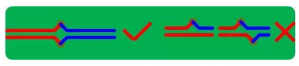
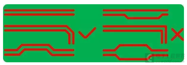
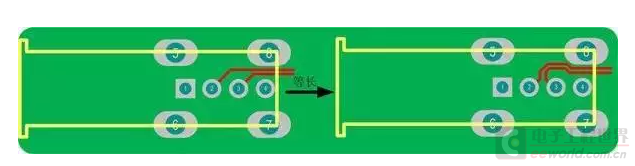
(1) differential traces must be of equal length, width, in close proximity, and the two lines at the same level.
If you wait long and equally not meet at the same time, the differential traces of PCB design is the most important rule is to match the line length. Meanwhile, in order to compensate for a matching impedance matching resistor may be added between the receiving terminal of the differential pair employed. Its value should be equal to the value of the differential impedance. Differential traces may take on different signal layers, but this is generally not recommended moves. Thus as little as possible cross-layer through holes and, as far as possible detours.
(2) between the differential pair have GND isolation, or to maintain the distance, not too close.
Increase the distance difference signal with the other signal traces, or by isolation GND.
(3) differential line routing priority
Fourth, give chestnuts
On (1) Hi3516A user manual, USB PCB Design Recommendations
In order to ensure good signal quality, USB 2.0 port trace data signal lines in a differential mode line. In order to achieve speed USB 2.0 high speed 480MHz, it is recommended for PCB layout using the following principles:
Differential data lines traces as short as possible, straight, internal differential data lines strictly equal length trace length, trace length deviation control within ± 5mil.
Differential data line control 90 ± 10% homogeneous differential impedance.
Differential data lines and does not want to change the alignment layer as a wiring layer in the ground plane adjacent traces.
Differential data lines traces ground plane layer should complete as reference plane, you can not cross the plane of division.
Differential data lines should traces vias and with a minimum of corners, or corner may be considered for an arc angle of 135 degrees, to avoid right-angle, to reduce reflection and impedance changes.
Avoid other high speed periodic signals near and current signals, and to ensure the spacing is greater than 50mil, to reduce crosstalk.
Moreover, non-periodic signal should be away from the low speed to ensure that the distance of at least 20mil.
REXT resistance should be as close as possible Hi3516A side.
(2) Description Graphic
See: the USB lessons routing the PCB - "Blood training"
USB is a fast, bidirectional, synchronous transmission, low-cost, easy to use hot-swappable serial interface. Since the data transmission speed, easy interface, support hot swap, etc. that the USB device is widely used. Currently, the market for the product to USB2.0 interface majority, but a lot of hardware newcomers encounter a lot of problems in USB applications, often after PCB assembly complete USB interface various problems
such as communication unstable or can not communicate, check the schematics and welding are no problem, perhaps this time would need to suspect that PCB design is unreasonable. Draw USB2.0 data transfer to meet the requirements of the PCB for product performance and reliability has a very important role.
USB protocol defined by the two differential signal lines (D +, D-) to transmit digital signals to USB devices stable differential signal lines must be strictly according to the rules of the differential signal layout. The USB I years experience related to the product design and debugging, the following summary of points to note:
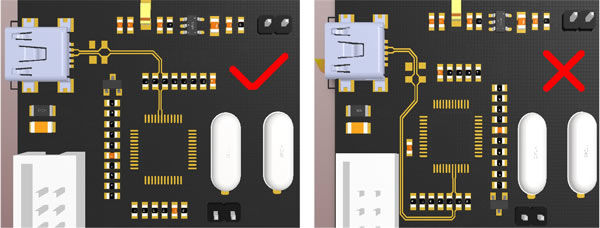
1. When component layout, the shortest possible wiring of the differential, the differential line traces to shorten the distance (√ reasonable manner, × unreasonable mode);
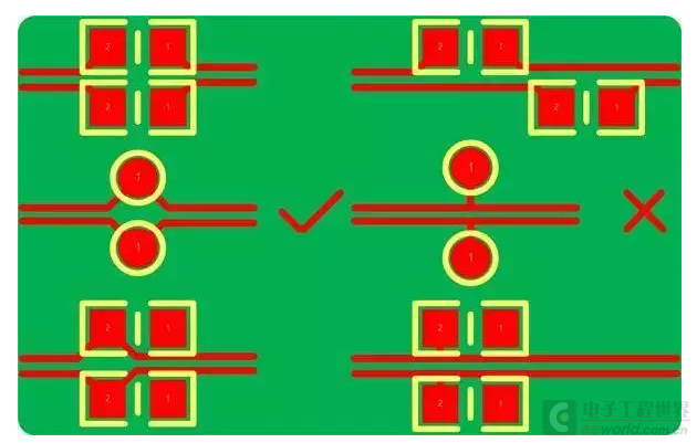
2. priority differential line drawing, a pair of differential lines so as not more than two pairs of through holes (vias increases the parasitic inductance of the line, so that affect signal integrity line), and the need to symmetrically placed (√ reasonable manner, × unreasonable manner);
3. parallel lines of symmetry, this will ensure that the two lines tightly coupled, to avoid traces 90 °, 45 ° or arc are preferred alignment manner (√ reasonable manner, as × unreasonable manner);
4. differential RC series, test points, placed on the pull-down resistor (√ reasonable manner, × unreasonable manner);
5. Since the distribution of pins, vias, traces and space the presence of such other factors is easy to mismatch the differential line length, and once the line length does not match the timing offset occurs, but also introducing a common-mode interference, reducing the signal quality. Therefore, to make the corresponding differential pair mismatch compensation, so that it matches line length, the length difference is usually controlled within 5mil, where there is a compensation principle where the length difference compensation;
Fifth, impedance matching
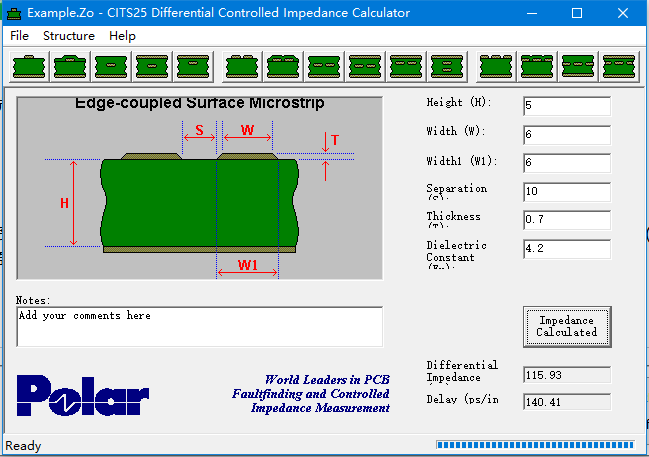
(1) impedance calculation tool
It has been mentioned above, the differential impedance. How this calculation it? Recommend a impedance calculation tool Polar CITS25
1, software download
举个例子:
我们用一对 0.006 英寸宽, 1/2 盎司铜厚,间距为 0.01 英寸, FR4 材料作衬底,离地线层 0.005 英寸 (微带方式)的差分信号走线的差分阻抗计算作为例子,铜的厚度 T 为 0.7/1000 英寸。下图显示了各参数。
(单位换算:1Mil=千分之一英寸,约等于0.0254毫米;1 盎司 = 0.0014 英寸=0.7 mil)
H:介质厚度(PP片或者板材,不包括铜厚) (5)
W:阻抗线下线宽(W2=W1-0.5MIL) (6)
W1:阻抗线上线宽(客户要求的线宽) (6)
S:阻抗线间距(客户原稿) (10)
T:成品铜厚 (0.7)
Er1:PP片的介电常数(板材为:4.5 P片4.2) (4.2)
2、软件各个界面含义
该软件跟上面软件不同,但是参数差不多,仅供参考。
如果想下载下面的软件,参看:PCB特征阻抗计算神器Polar SI9000安装及破解指南
1. 外层单端:Coated Microstrip 1B
H1:介质厚度(PP片或者板材,不包括铜厚)
Er1:PP片的介电常数(板材为:4.5 P片4.2)
W1:阻抗线上线宽(客户要求的线宽)
W2:阻抗线下线宽(W2=W1-0.5MIL)
T1:成品铜厚
C1:基材的绿油厚度(我司按0.8MIL)
C2:铜皮或走线上的绿油厚度(0.5MIL)
Cer:绿油的介电常数(我司按3.3MIL)
Zo:由上面的参数计算出来的理论阻值
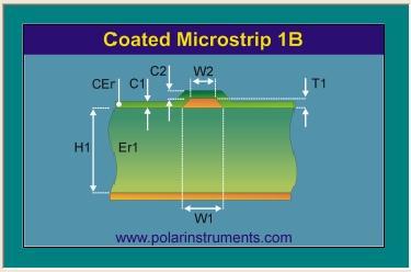
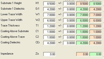
2.外层差分:Edge-Coupled Coated Microstrip 1B(重点)
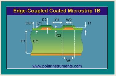
H1:介质厚度(PP片或者板材,不包括铜厚)
Er1:PP片的介电常数(板材为:4.5 P片4.2)
W1:阻抗线上线宽(客户要求的线宽)
W2:阻抗线下线宽(W2=W1-0.5MIL)
S1:阻抗线间距(客户原稿)
T1:成品铜厚
C1:基材的绿油厚度(我司按0.8MIL)
C2:铜皮或走线上的绿油厚度(0.5MIL)
C3:基材上面的绿油厚度(0.50MIL)
Cer:绿油的介电常数(我司按3.3MIL)
3.内层单端:Offset Stripline 1B1A
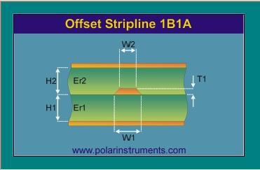
H1:介质厚度(PP片或者光板,不包括铜厚)
Er1:H1厚度PP片的介电常数(P片4.2MIL)
H2:介质厚度(PP片或者光板,不包括铜厚)
Er2:H2厚度PP片的介电常数(P片4.2MIL)
W1:阻抗线上线宽(客户要求的线宽)
W2:阻抗线下线宽(W2=W1-0.5MIL)
T1:成品铜厚
Zo:由上面的参数计算出来的理论阻值
4.内层差分:Edge-Couled Offset Stripline 1B1A
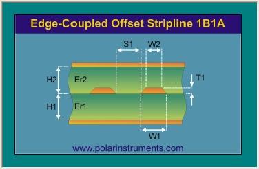
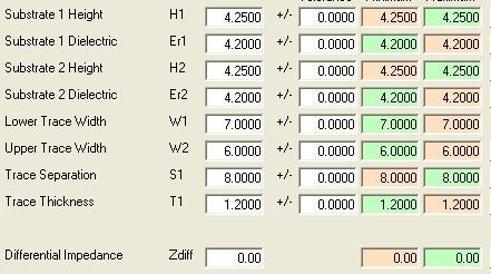
H1:介质厚度(PP片或者光板,不包括铜厚)
Er1:H1厚度PP片的介电常数(P片4.2MIL)
H2:介质厚度(PP片或者光板,不包括铜厚)
Er2:H2厚度PP片的介电常数(P片4.2MIL)
W1:阻抗线上线宽(客户要求的线宽)
W2:阻抗线下线宽(W2=W1-0.5MIL)
S1:客户要求的线距
T1:成品铜厚
Zo:由上面的参数计算出来的理论阻值
5.外层单端共面地:Coated Coplanar Waveguide With Ground 1B
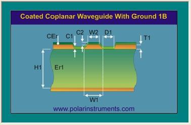
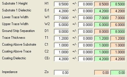
H1:介质厚度(PP片或者板材,不包括铜厚)
Er1:PP片的介电常数(板材为:4.5 P片4.2)
W1:阻抗线上线宽(客户要求的线宽)
W2:阻抗线下线宽(W2=W1-0.5MIL)
D1:阻抗线到两边铜皮的距离
T1:成品铜厚
C1:基材的绿油厚度(我司按0.8MIL)
C2:铜皮或走线上的绿油厚度(0.5MIL)
Cer:绿油的介电常数(我司按3.3MIL)
Zo:由上面的参数计算出来的理论阻值
6.外层差分共面地:Diff Coated Coplanar Waveguide With Ground 1B
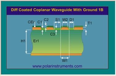
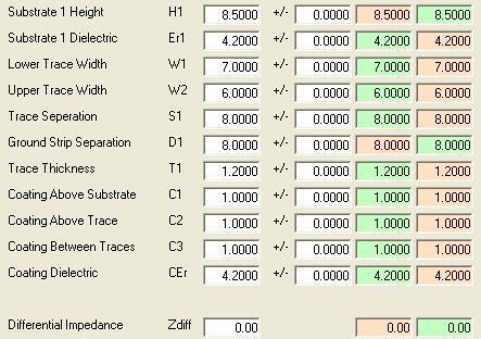
H1:介质厚度(PP片或者板材,不包括铜厚)
Er1:PP片的介电常数(板材为:4.5 P片4.2)
W1:阻抗线上线宽(客户要求的线宽)
W2:阻抗线下线宽(W2=W1-0.5MIL)
S1:阻抗线间距(客户原稿)
D1:阻抗线到铜皮的距离
T1:成品铜厚
C1:基材的绿油厚度(我司按0.8MIL)
C2:铜皮或走线上的绿油厚度(0.5MIL)
C3:基材上面的绿油厚度(0.50MIL)
Cer:绿油的介电常数(我司按3.3MIL)
Zo:由上面的参数计算出来的理论阻值
(2)阻抗匹配
参看:PCB阻抗设计参考
参看:PCB迹线的阻抗控制技术
参看:PCB阻抗匹配总结
确实,一开始我也以为阻抗是写到 PCB 制版要求里,然后让制版厂来做的。
从上面的例子中就可以看到它与 差分线的线宽、线间距、介质厚度、成品铜厚、介电常数、叠层结构 等有关。
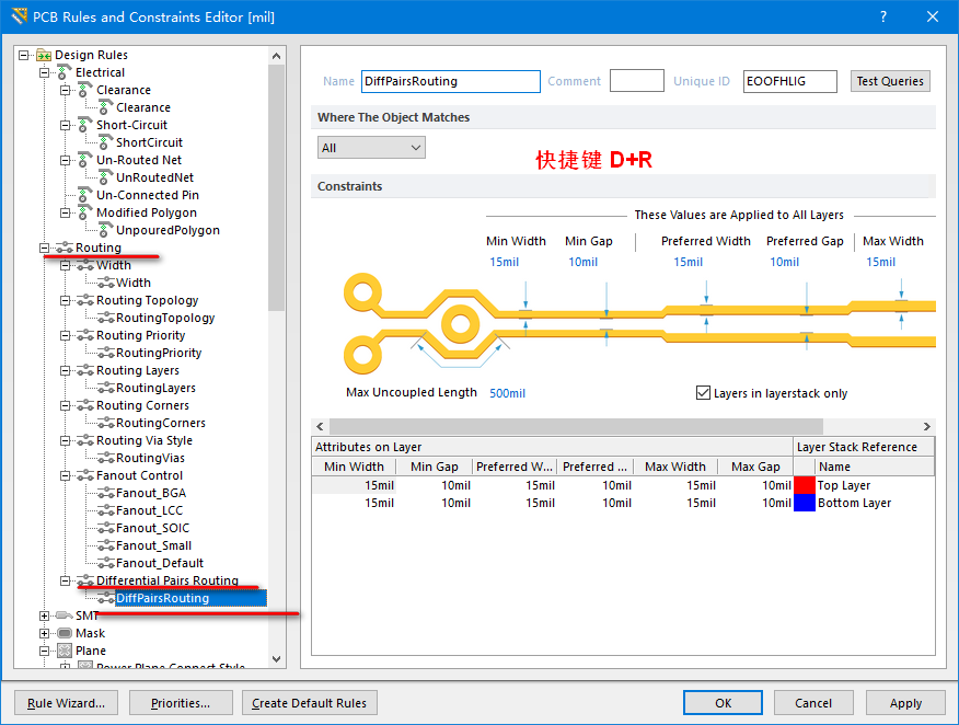
差分线的线宽、线间距,这些都是在 PCB 规则里设置好的。只不过以前不晓得,为什么要设置成线宽 6 mil,间距 8 mil 等等这样的要求,还以为只是与制版价格有关呢。现在看来,它还和阻抗大小有关的!!
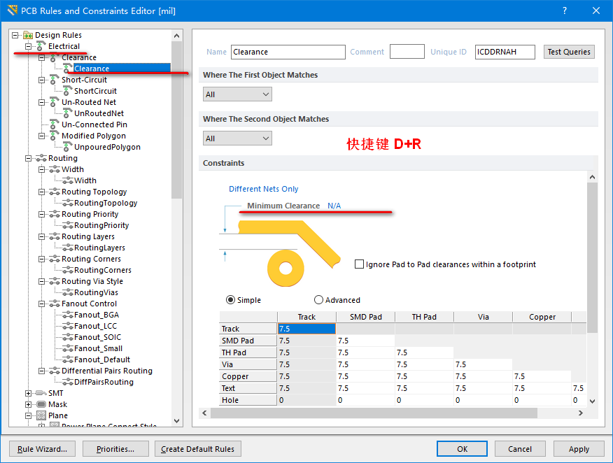
1、线宽、线间距规则设置
线宽:(最小线宽 5mil)
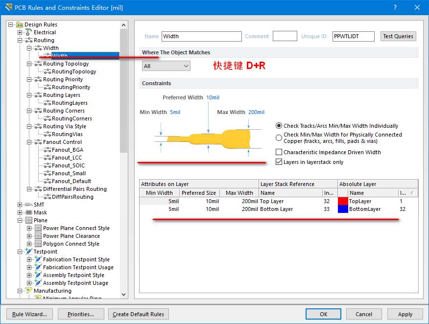
差分线间距:(差分线最小间距 10mil)
其他信号线间距:(最小线宽 7.5mil)
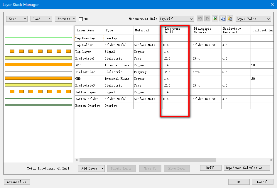
2、查看板卡厚度和叠层结构
在 Design--Layer Stack Manager--thickness
(3)传输线阻抗计算中的有关问题
上面参看的文档,讲的真好,看了一遍受益匪浅。不过内容较多,不一一分析了,下面只看一部分。
结合目前我公司 PCB 板加工厂家的工艺能力,在用 polar 公司阻抗计算器 CITS25 计算PCB 板上迹线特性阻抗时,对影响 PCB 板迹线控制阻抗的几个相关参数分述如下:
1、 铜层厚度
铜层厚度代表了 PCB 迹线的高度 T。内层铜箔通常情况下用到 1 OZ(厚度为 35 微米),也有在电源层要流过大电流时用到 2OZ(厚度为 70 微米)。外层铜箔常用 1/2 OZ(18 微米),但由于经过板镀和图形电镀最终成品外层铜厚将达到48 微米(实际计算时用该值),设计成其他铜厚将较难控制铜厚厚度公差。若外层使用 1OZ铜箔,则最终铜厚将达到 65 微米。
2、 PCB 板迹线的上下线宽
由于侧蚀的影响, PCB 迹线的截面为一梯形,上下线宽差距以 1mil 来计算,其中下线宽=要求线宽,而上线宽=要求线宽-1mil。
3、 阻焊层
阻焊层厚度按 10um 为准(选择盖阻焊模式),但有机印后将会有所增厚,但其变化将基本不会带来阻抗值的变化。
4、 介质厚度
常用板材(芯板): (mm OZ/OZ *表示其数值为不包括铜箔厚度的芯板厚度)
0.13* 1/1 0.21* 1/1 0.25* 1/1 0.36* 1/1
0.51* 1/1 0.71* 1/1 0.80* 1/1
1.0 1/1 1.2 1/1 1.6 0.5/0.5 1.6 1/1 1.6 2/2
2.0 1/1 2.0 2/2 2.4 1/1 3.0 1/1 3.2 1/1
芯板在计算控制阻抗时的实际厚度:

常用半固化片: (mm/mil)
7628: 0.175/6.9
2116: 0.11/4.3
1080: 0.066/2.6
实际计算厚度时注意半固化片随着两面线路结构不同而有所不同:(mil)
其中 GND 层包括铜面积占 80%以上的线路层。如果介质在 HOZ 和 1OZ 铜箔之间,其厚度按 HOZ 情况计算。
5、 介电常数
● Er 的值是线路板材质的绝缘常数(介电常数), 它对于线路的特性阻抗值而言是一个重要的组成部分。设计厂商因此有时会指定迹线阻抗值并依赖于线路板制造商来控制流程,以使迹线阻抗满足设计厂商指定的技术规范。
● 迹线的控制阻抗与板材介电常数的平房根成反比。
● 通过板材供应商提供的板材阻抗范围为 4.2~5.2,而 POLAR 公司建议单端采用 4.2,而差分若两线间距小会有所影响则建议采用 4.7。
● 根据一年多来各阻抗实验及生产板,我公司选用 4.2 进行计算能符合要求。
● 由于介电常数与板材型号和信号频率有相关性, 请设计人员能充分考虑该影响。如:高频板材有介电常数 2.5 等。
(4)传输线阻抗控制典型应用总结
我们的制版要求,如果需要差分阻抗,一般会有这几个选项:
层数:4
板厚1.6mm,整板喷锡工艺。
阻抗匹配 目录中的图片信号需要100欧姆差分阻抗匹配。
严格禁止修改PCB图的任何东西的。
则 1.6mm 厚度的 4 层 PCB 板加工,建议做阻抗设计的时候按照 1.5mm 厚度进行设计,剩下 0.1mm 厚度留给工厂作为其他工艺要求用(后制诚厚度,绿油、丝印等)。
板厚 1.5mm(采用 1.2 35/35 的芯板,其余两个介质层为 2116)。
L1/L4 层差分信号(阻抗控制为 100Ω)的线宽/间距可以为 5/5、 5/6、 6/7、 6/8、 6/9(mil/mil)
L1/L4 层差分信号(阻抗控制为 75Ω)的线宽/间距可以为 10/7、 10/6、 11/9、 11/10、10/11(mil/mil)①
计算单端阻抗和差分阻抗的界面分别如下图一和图二:
L1 和 L2 层、 L3 和 L4 层之间的介质层用 2116,模式为 Copper/Gnd(HOZ), 所以 厚度 H=4.6mil,介电常数为 4.5,外层铜厚为 1OZ(1.9mil)。
实际板厚: 0.01+0.048+0.12+1.2+0.12+0.048+0.01=1.556mm。②
注 1:此处差分信号表示方式线宽/间距中的间距指的是两条差分线内侧边到边的距离,在 Allegro 中设置布线规则中也使用内侧边到边的距离, 但在有些参考中用的是两条差分线中心到中心的距离, 在应用时要注意加以区别。 例: 8/8(mil/mil)的差分线如果间距是用内侧边到边的距离表示,则差分线中心到中的间距表示为 8/16(mil/mil)。
注 2: 实际板厚计算中 0.01 代表的时 PCB 板表面的阻焊层, 阻焊层不会影响控制阻抗,单会影响 PCB 板的整体厚度。
其他层自行查看,不过层结构值得看一下:
四层板:最常用的信号叠层顺序为 Sig/Gnd/Power/Sig
六层板:较容易实现阻抗控制的的信号叠层顺序为 Sig/Gnd/Sig/Sig/Power/Sig
六层板:还有一种结构不对称的叠层顺序经常用道: Sig/Gnd/Sig/Gnd/Power/Sig
八层板:对称结构Sig/Gnd/Sig/Gnd/Power/Sig/Gnd/Sig
十层板:信号顺序 Sig/Gnd/Sig/Sig/Gnd/Gnd/Sig/Sig/Gnd/Sig(结构对称)
十二层板:信号顺序Sig/Gnd/Sig/Gnd/Sig/Gnd/Gnd/Sig/Gnd/Sig/Gnd/Sig
或参看:Altium Designer -- PCB 叠层设计
(5)总结
阻抗计算参数与阻抗影响关系:
1. H介质层厚度 H与Zo成正比,H值越大,Zo越大; 2. W1线宽 W1与Zo成反比,W1值越大,Zo越小; 3. T 铜厚 T与Zo成反比,T值越大,Zo越小; 4. Er 介电常数 Er与Zo成反比,Er值越大,Zo越小; 5. S差动阻抗线间距 S与Zo成正比,S值越大,Zo越大;
主要通过下面的途径对阻抗设计进行微调:
◆ 调整阻抗控制线宽、间距; ◆ 调整介质层厚度。
总结:
阻抗控制线宽、间距、叠层结构,这些是硬件工程师在 PCB 设计时设置的,一般制版时要求严格禁止修改PCB图的任何东西的。至于介电常数、介质厚度、成品铜厚,这些是与材质有关,这就是PCB 加工厂家的事了。
