DCDC power supply PCB layout
Although the switching power supply has many advantages such as high efficiency and wide dynamic range, it also brings more serious switching interference. If these interferences do not take certain measures to suppress, eliminate and shield, it will seriously affect the normal operation of the whole machine. First-tier manufacturers like Maxim provide design tools to help customers speed up the design process. This video is their suggestion for PCB layout. The video will introduce the rules of the DC-DC power supply PCB layout from the principle level, so as to prevent everyone from falling into various pits when developing.
Unreasonable PCB layout may cause a series of problems, such as:
Low conversion efficiency leads to high heat generation of components;
unstable drive waveform;
EMI problem;
output ripple exceeds the standard;
more serious IC does not work or even burns directly
. Take the Buck circuit as an example. The circuit is divided into a small signal control circuit and a large current power circuit. First, in order to avoid interference of the control signal, the control circuit and the power circuit need to be arranged separately; secondly, the power circuit with high current needs to be arranged first.
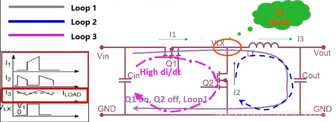
As can be seen from the figure above, the voltage waveform of the LX node is a square wave, and the currents I1 and I2 passing through Q1 and Q2 are similar to square waves. They all contain high-frequency harmonics, which are noise sources that we need to focus on; The current is a triangular wave and a noise source that cannot be ignored.
The more important one is the layout of components on the Loop 3 loop. Loop 3 loop current has a sudden change, that is, a higher di/dt; the parasitic inductance of the PCB lead on this loop will cause a larger voltage spike. So we have to reduce the loop area of Loop 3 as much as possible, and use the thickest possible trace to reduce parasitic inductance.
In addition, without significantly affecting the efficiency, the rise and fall time of the LX node voltage should be extended as much as possible to facilitate the reduction of high frequency harmonics. It is recommended to reserve an RC snubber absorption circuit at the LX node. Generally, a resistance of ~2ohm is selected, and then the capacitance is adjusted to match the actual circuit. Considering the impact on efficiency, the capacitance generally does not exceed 330pF. Under ideal conditions, the loss of the RC snubber absorption circuit should offset the energy storage loss of the parasitic element before adding it to ensure that the rise and fall time of the LX node are prolonged without increasing the loss.
The following Loop 2 loop also needs to adopt the same strategy: reduce the loop area as much as possible to suppress noise emission.
For externally compensated DCDC converters, the compensation circuit should be as close as possible to the converter, and short leads should be used to keep away from the power signal, so as not to affect the stability of the system.
1. Basic principles of wiring
Input power supply and output power supply need to be isolated by GND and avoid parallel wiring;
power circuit and control circuit need to be arranged in different areas to avoid overlap;
low-frequency signal lines should be kept away from high-frequency signal lines;
high di/dt and dv/dt wiring should be avoided May be short
2. Line width principle
The line width is determined by the magnitude of the current flowing. Large current traces should provide sufficient line width to optimize efficiency and reduce heat generation; especially for the LX node, copper can be used under conditions.
The line width of the control circuit is at least 20mil, such as Vcc, AGND (SGND); in order to reduce the impedance of the gate drive signal (DH, DL), it is recommended to use a line width of 25mil; other signal lines have a width of at least 10mil;
3. Bypass/decoupling capacitor
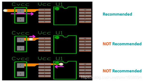
The capacitor is placed close to the IC power supply pin;
when there are multiple capacitors, the small value is close to the IC; the
capacitor layout position
4. Via
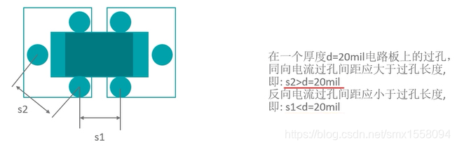
The current direction is the same: the center distance between the vias should be greater than the length of the via; the
current direction is opposite: the center distance between the vias should be less than the length of
the via ; the position of the via VIa
5. Grounding method
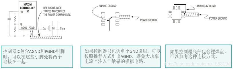
Single point grounding The
analog ground and digital ground need to be connected at a single point.
6. Thermal design
Provide enough copper around the MOSFET and inductor to improve heat dissipation; increase via holes and use exposed pads to improve circuit board heat dissipation.
7. Inductance design
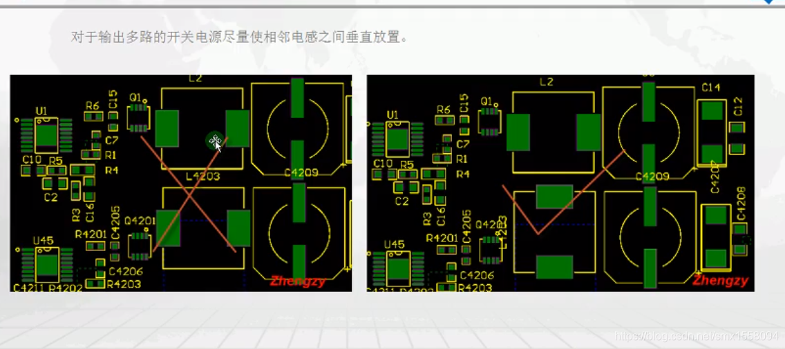
For switching power supplies with multiple outputs, try to place adjacent inductors vertically