Meet the requirements of manufacturability, assemblability and maintainability, convenient for inspection and repair during debugging, and easy to disassemble components:
1) There should be no more than two directions for polar devices, and it is best to carry out requirements such as uniform directions, as shown in Figure 1-1;
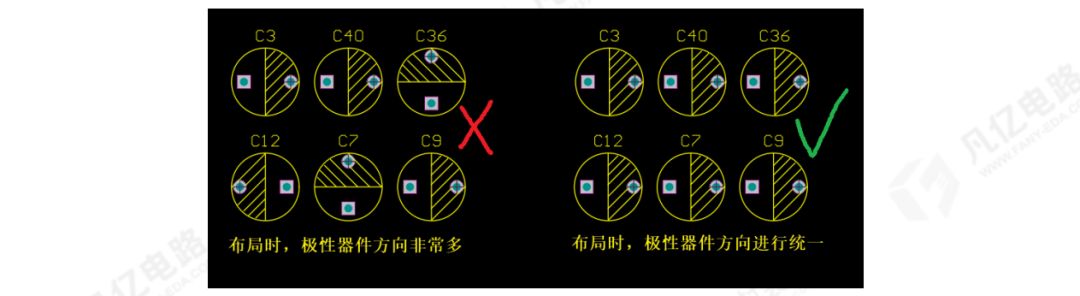
Figure 1-1 Uniform placement of polar devices
2) The curved/male and curved/female crimping connectors are on the same surface as the crimping parts. No high devices (greater than 3mm) shall be placed within 3mm around the crimping parts, and any welding parts shall not be arranged within 1.5mm around the crimping parts. No components shall be placed within 2.5mm from the pins of the crimping parts on the back of the crimping parts, as shown in Figure 1-2.
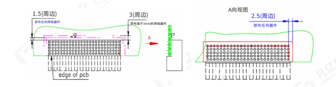
Figure 1-2 Prohibited layout of bend/male and bend/female crimp connection components
3) Straight/male and straight/female crimping connectors shall not have any components arranged within 1 mm of the crimping device. When a sheath needs to be installed on the back, no components shall be arranged within 1 mm of the surrounding area. When the sheath is not installed, the distance between the crimping parts No components shall be placed within 2.5mm of the pin, as shown in Figure 1-3.
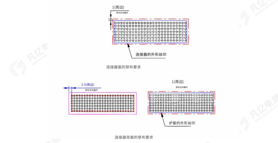
Figure 1-3 Straight/male, straight/female crimp connector layout forbidden area
1) For conventional post-soldering devices (connectors), when the layout is on the same layer, the distance between the device and the connector is guaranteed to be 1.5mm and above. Try not to arrange SMD devices within 3mm of plug-in devices or board edge connectors to prevent stress damage to devices when connectors are plugged in and out, as shown in Figure 1-4.

Figure 1-4 Layout of plugging and unplugging devices
5) BGA devices: The devices on the same plane are laid out 5mm away from the periphery of the BGA device. In the case of crowded space, the devices on the same plane can also be laid out 3mm away, as shown in Figure 1-5.
6) The back layout of the power supply filter capacitor of the BGA device should be as close as possible to the corresponding power supply pin layout, and the layout should be on the symmetrical center of the two adjacent pads of the BGA (some customers require: do not cover the pads of the BGA, avoid making X The pads of the BGA cannot be irradiated during radiographic inspection). As shown in Figure 1-6.
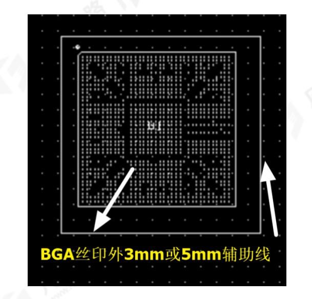
Figure 1-5 BGA peripheral layout range
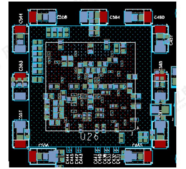
Figure 1-6 Capacitor layout on the back of the BGA
7) Double-sided layout of BGA devices. Generally, BGA devices are not allowed to be placed on the back side. When there are BGA devices on the back side, BGA devices cannot be placed within the projection range of 8mm around the front BGA device, as shown in Figure 1-7.
8) Double-sided layout devices, unless there are special requirements, large devices and chips are placed on the TOP layer, and 0805, 0603, 0402 resistor containers are placed on the back, as shown in Figure 1-8.
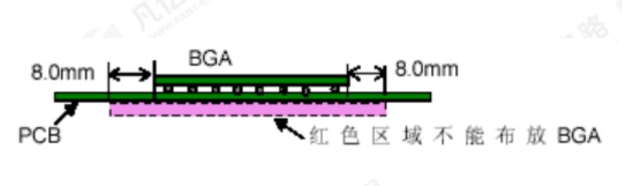
Figure 1-7 BGA rear area layout
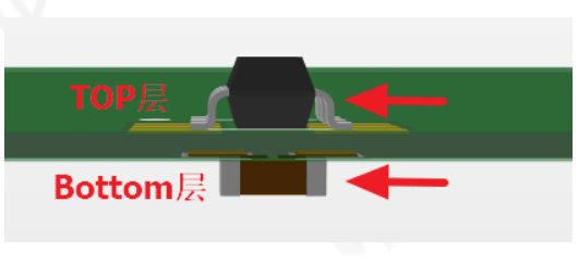
Figure 1-8 Layout of top and bottom devices
9) Small components (resistors, capacitors and Chip devices) should not be surrounded by tall devices, and there must be enough space (at least 3mm left and right) for easy disassembly, as shown in Figure 1-9 and Figure 1-10. The layout principles of high and low components , the tall devices are arranged behind the low devices and arranged along the direction of the least wind resistance to prevent the air duct from being blocked.
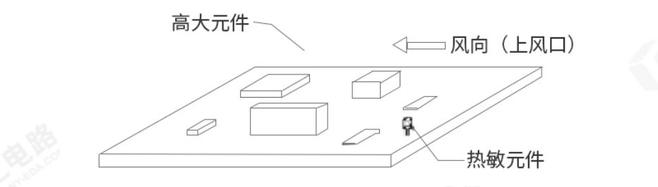
Figure 1-9 Schematic diagram of device layout requirements
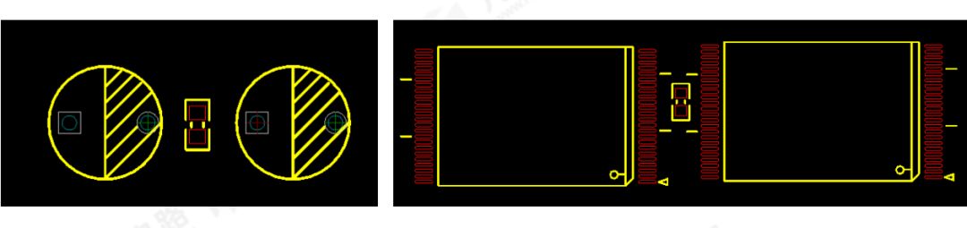
Figure 1-10 Chip device layout surrounded by high devices
10) For metal shell devices, metal parts with different properties (such as heat sinks, shields) or metal shell devices cannot touch each other to ensure that they do not collide with other devices and ensure that the minimum distance of 1mm meets the installation space requirements, as shown in Figure 1 -11 shown.
11) The recommended device layout direction is 0°, 90°, unless special circumstances, please do not place it at 45°, as shown in Figure 1-12.
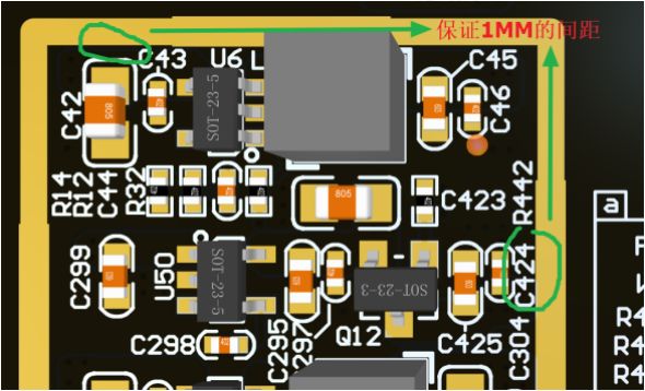
Figure 11 The distance between the device and the shield is 1mm
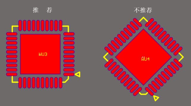
Figure 1-12 Device placement angle
12) There must be an operable space between devices (such as obliquely inserted memory sticks) to facilitate operations such as plugging and unplugging, as shown in Figure 1-13.
13) Layout of PCBs with windows For PCBs with window requirements, ensure that there is a distance of at least 2 mm between the device and the window during layout, as shown in Figure 1-14.
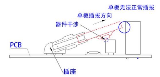
Figure 1-13 Spacing operation space reserved for devices and devices
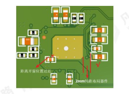
Figure 1-14 Layout spacing requirements between devices and window openings
14) If there is no SMT device within 5mm of the board edge, the 5mm transmission edge can be omitted to save the board, but if there is, it is directly recommended that the customer add a process auxiliary edge; generally the long side is used as the transmission edge, and the ratio of the short side to the long side is greater than 80% , the short side can also be used as the transmission side. When the device layout cannot meet the requirements of the width of the transmission edge (the board edge is 5mm forbidden), the method of adding auxiliary edges should be used. The general requirements for adding the width of the auxiliary side: the width of the auxiliary side of the PCB that does not need to be assembled is 5mm, and the width of the auxiliary side of the PCB that is assembled is at least 8mm. If the stamp hole imposition method is used, please pay attention to the parameter setting of the stamp hole.
15) When delivering, be sure to check the layout of Mark points, whether the number is sufficient, and whether the distance from the edge of the board is more than 5mm, as shown in Figure 1-15.
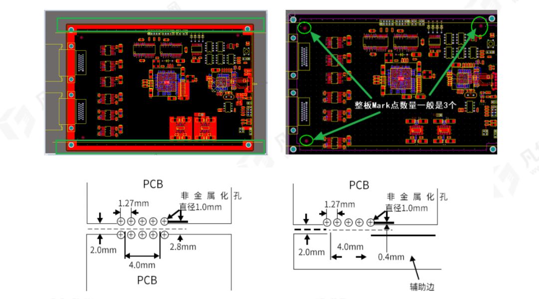
Figure 1-15 Parameter setting of stamp hole imposition
Disclaimer: This article is an original article by Fanyi Education, please indicate the source for reprinting!