Basic timing path constraints
0. Overview
The RTL code describes the sequential logic and combinational logic of the circuit, that is, the RTL code embodies the register structure and number of the circuit, the topological structure of the circuit, the combinational logic function between registers, and the combinational logic function between registers and I/O ports. But the code does not include the circuit time (path delay) and circuit area (the number of gates), so these need to be restricted.
Synthesis tools cannot support asynchronous circuits well, or even asynchronous circuits. Therefore, the timing path constraints are mainly for synchronous circuits . Regarding the constraints of asynchronous circuits, this article will not introduce them in detail.
Timing constraints can be very complicated. Here we first introduce the basic timing path constraints.
1. Timing path and critical path
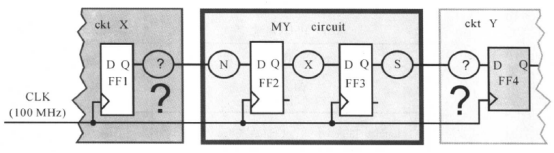
The common structure of the synchronization circuit is as follows:
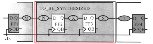
In the middle is the designed module (chip) . For the synchronous circuit, in order to make the circuit work normally, that is, the circuit can function correctly under the specified operating frequency and working environment, all timing paths in the design need to be restricted.
The timing path is a point-to-point data path, and data is transmitted along the timing path. Each timing path has a start point and an end point.
The starting point is defined as: (1) input port; (2) clock pin of flip-flop or register.
The end point is defined as: (1) output port; (2) all input pins of sequential devices except clock pins.
The timing path can be input port to register, register to register, register to output port, input port to output port.

There are 4 paths in the figure:
1: From input port A to D of FF1;
2: From CLK of FF1 to D of FF2;
3: From CLK of FF2 to output port out1;
4: From input port A To output port out1.

The path is characterized by delay, that is, paths 1, 2, 3, and 4 all have delays. The path with the longest delay is called the critical path . In general, paths 1, 2, and 3 are the most common, and path 4 is relatively rare.
2. Common timing path constraints
Setup time, hold time, metastable state
The setup time (setup time) refers to the time when the data is stable before the rising edge of the clock signal of the flip-flop arrives. If the setup time is not enough, the data will not be input to the flip-flop on the rising edge of the clock;
hold time It refers to the time when the data is stable after the rising edge of the clock signal of the flip-flop arrives. If the retention time is not enough, the data cannot be output stably from the flip-flop.

The metastable state means that the output terminal of the flip-flop cannot reach a confirmable state within a certain period of time, and it is neither a high level nor a low level state. When the flip-flop is in this state, the subsequent combinational logic may be in an oscillating state, and this state may be cascaded along the various flip-flops on the signal path.
The constraint is to satisfy the setup time (and hold time) of the register .
Constraints on path 2 (register-register)
For path 2, the data transmission from the D port of FF1 to the D port of FF2 mainly needs to experience the flip time/conversion delay of the flip-flop, the combined logic delay between the register and the register, and the wiring delay. Because the data is transmitted back by the beat of the clock, the path constraint between the register and the register here is the modeling of the clock, or the constraint on the clock .

The delay time of path 2 should satisfy: Tcomb< Tclk-Tclk-q-Tsetup
where Tclk-q is the delay from pin CLK to pin Q of FF2, and Tsetup is the setup time of FF3. Both of these parameters are determined by the process Library provided.
The command to define the clock is: create_clock. Assuming the clock cycle is 10ns, the command to define the clock is:
create_clock -period 10 [get_ports clk]
The corresponding clock waveform is:

When defining the clock (except for the virtual clock, which will not be introduced for the time being), the clock period (that is, the -period option) and the clock source (port or pin) (that is, the clk in the design ) must be defined , and some You can use options to define the duty cycle, offset/skew and clock name of the clock. You can use man create_clock to view the relevant options of the command.
Once the clock is defined, the path between the registers has been restricted. You can use the report_clock command to view the defined clock and its attributes. If you need to use both edges of the clock (rising edge and falling edge), the duty cycle of the clock will affect the timing constraints.
It is obviously too ideal to define only one clock cycle to constrain the path between the register and the register. You need to add other clock attributes. Before adding, you need to know the clock's skew, jitter, and conversion time. The concepts of (transition), latency (latency), or the attributes of these clocks, and more specific clock constraints can be found in this blog post: http://www.cnblogs.com/IClearner/p/6440488.html The modeling of the clock is introduced in detail, that is, the constraint of path 2.
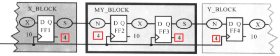
Constraints on path 1 (input-register)
Assume that the same clock CLK is used before and after the module, as shown in the figure below. (We will not discuss the use of different clocks for the time being)
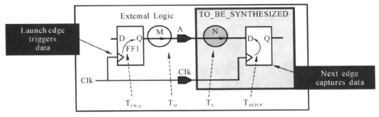
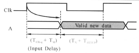
In the above figure, on the rising edge of the Clk clock, the data sent through the register FF1 of the external circuit is transmitted to the circuit to be synthesized through the input port A, and is received by the internal register FF2 on the rising edge of the next clock. The timing relationship between them is shown in the following figure:
For the module to be integrated, the combination logic of the DC integrated input, that is, the circuit N above, the delay to get it is Tn, but does this Tn meet the requirements (for example, meet the setup time of the flip-flop)? Before constraining, DC does not know, so by constraining this path, it is to tell the external delay of DC (including register flip delay and combinational logic, transmission delay of line network), for example, Tclk -q+Tm, after constraining the clock, DC will calculate the delay left by this path for circuit N, which is Tclk-q+Tm. Then DC compares Tclk -(Tclk-q+Tm) with Tn+Tsetup to see if Tclk -(Tclk-q+Tm) is greater than Tn+Tsetup, that is, to see if the delay Tn of the integrated circuit N is It is not too large. If Tn is too large, greater than Tclk -(Tclk-q+Tm), then DC will be optimized to reduce delay. If the delay is still too large, DC will report an error. Therefore, it is necessary to constrain the input port and tell the delay of the external circuit so that the DC constrains the input combinational logic.
If the delay of the external circuit of the input port is known (assumed to be 4 ns, including the flip delay and the external logic delay), the maximum allowable delay from the input of the integrated circuit to the register N can be easily calculated:

In DC, use the set_input_delay command to restrict the delay of the input path:
set_input_delay -max 4 -clock CLK [get_ports A]
It specifies how much time the external logic uses, and how much time is left for the internal logic in the DC calculation. In this command, the external logic uses 4 ns. For a circuit with a clock cycle of 10 ns, the maximum delay of the internal logic is 10-4-Tsetup = 6-Tsetup.
When the input combinational logic has multiple input ports, as shown in the figure below:

You can use the following commands to set constraints on all input ports except the clock:
set_input_delay 3.5 -clock Clk -max [remove_from_collection [all_ inputs ] [get_ports Clk] ]
If you want to remove multiple clocks, use the following command:
Remove_from_collection [all_inputs] [get_ports "Clk1 Clk2"]
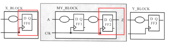
Constraints on path 3 (register-output)
Path 3 is similar to Path 1, assuming that the registers connected to the output terminals use the same clock CLK.
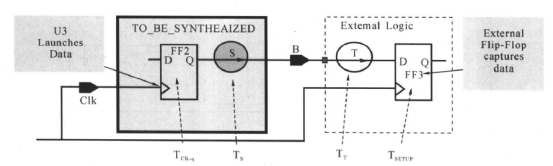
The rising edge of the clk clock sends data through the register FF2 of the internal circuit through the circuit S to be synthesized, and reaches the output port B. At the rising edge of the next clock, it is received by the FF2 of the external register. The timing relationship between them is shown in the following figure.

To constrain the delay of the combined path circuit S and let DC calculate whether its delay can satisfy the timing relationship, it is necessary to tell the approximate delay of the external output of the DC.
When the delay of the external circuit is known (assumed to be 5.4 ns), the maximum delay left for the output port of the integrated circuit can be easily calculated, as shown in the following figure:

In DC, use the set_output_delay command to restrict the delay of the output path. For the above circuit diagram, there are:
set_output_delay -max 5.4 -clock Clk [get_ports B]
It specifies how much time the external logic uses, and how much time is left for the internal logic in the DC calculation. In this command, the external logic uses 5.4 ns. For a circuit with a clock cycle of 10 ns, the maximum delay of the internal logic is 10-5.4-Tclk-q = 4.6-Tclk-q.
Note: General constraints for paths 1, 2, and 3
In the SOC design, due to the relatively large circuit, the design needs to be divided. In a design team, each designer is responsible for one or several modules . The designer often does not know the external input delay and/or external output establishment requirements of each module (these requirements may be written in the design specification, or not, the designer will not know when there is no), as shown in the figure below Shown:
At this time, you can set up timing constraints for the input/output ports by establishing a time budget (Time Budget), that is, preset these delays first, and everyone will discuss it first (or the design specification declares it). But how many presets are appropriate? There are the following basic principles:
(1) It can be assumed that the internal circuit of input and output only uses 40% of the clock cycle . If all modules in the design constrain the input/output according to this assumption, there will be 20% of the clock cycle time as the margin (Margin). The margin includes the delay of register FF1 and the setup time of FF2. That is: the margin = 20%*Tclk-Tclk-q-Tsetup, as shown in the figure below.

Example:
The constraints corresponding to the circuit above are:
create_clock  -period 10  [get_ports CLK]
set_input_delay  -max 6  -clock CLK  [all_inputs]
remove_input_delay  [get_ports CLK]  ;#时钟不需要输入延迟的约束
set_output_delay  -max 6  -clock CLK  [all_outputs]
(2) The module is divided by the output of the register , the time budget will become simpler
The constraints corresponding to the circuit above are:
set Tclk_q 1  ;#设置Tclk_q为1ns
create_clock  -period 10  [get_ports CLK]
set_input_delay  -max $Tclk_q  -clock CLK  [all_inputs]
remove_input_delay  [get_ports CLK]  ;#时钟不需要输入延迟的约束
set_output_delay  -max [expr 10-$Tclk_q]  -clock CLK  [all_outputs]
Constraints on path 4 (combination logic)
There are two situations in the path of combinational logic:
(1) In addition to the combinational logic from input port to output port in the module, there is also sequential logic, that is, there is a clock in the module;
(2) Pure combinational logic module, there is no clock inside the module.
The second case requires the use of the concept of a virtual clock. I will not introduce it for now, but only introduce the constraints of the first case. For example, the circuit in the figure below:
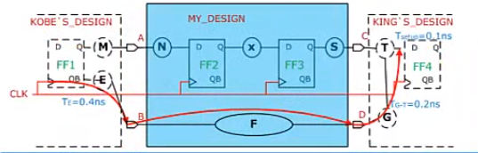
The delay Tf of the combinational logic part F is equal to Tclk-Tinput_delay-Toutput_delay. The clock cycle minus the two ends, and the intermediate delay constraint is obtained. The constraints are as follows:
set_input_delay  0.4  -clock CLK  -add_delay [get_ports B]
set_output_delay  0.2  -clock CLK  -add_delay [get_ports D]
set_max_delay   $CLK_PERIOD  -from [get_ports B]  -to  [get_ports D]  ;#这条约束可有可无
3. Examples of timing constraints
On the basis of DesignCompiler Learning (3)-Basic Operation Process article, modify the ./scripts/top.con constraint file to the following content:
current_design Adder

# Reset all constraints
reset_design


create_clock  -period 10  [get_ports clk]
set_input_delay  -max 6  -clock clk  [all_inputs]
remove_input_delay  [get_ports clk]
set_output_delay  -max 6  -clock clk  [all_outputs]
Start synthesis:
[IC@IC lab1]$ dc_shell -topo

dc_shell-topo> read_file -format verilog ./rtl/top.v # 读入设计
source ./scripts/top.con # 约束设计
compile_ultra # 这是在拓扑模式下进行综合的命令
report_qor > qor.report # 生成report信息并保存在qor.report文件中
report_timing # 查看时序报告