Entering the next semester of junior year, while preparing for the postgraduate entrance examination, I also intend to organize and expand the skills learned. At that time, whether it is through the preliminary examination of the postgraduate entrance examination and then participates in the re-examination or fails the postgraduate entrance examination to find a job, it will be useful.
I recently saw the world-class courses of UCSD (University of California) on the digital circuit, and I was shocked, so I plan to start here, but this tutorial is still outline, and I won’t explain everything I use. , But I will tell you what knowledge is needed.
This series intends to open the following chapters:
Combinatorial logic and synchronous timing design
Asynchronous timing circuit design actual combat: 16-person voting machine (self-made circuit after
multisim simulation) FSM (finite state machine) and HLSM (advanced state machine) (board experiment)
Memory and their Verilog implementation (simulation and board experiment)
AD/DA conversion and their Verilog implementation (simulation and board implementation)
Of course, I will change some of these things according to my needs. For example, I will do it according to the requirements of my RF system learning for ADC. Please look forward to it.
1. Combinational logic circuit
Combinational logic circuit refers to a digital circuit whose input determines output and has no memory (no storage function, the state of the previous moment does not affect the state of the next moment).
To master the basic knowledge required for the design of combinational logic circuits: basic gate circuits (and, or, not and their combined operations) and their operational relations, Boolean algebra used in digital circuits (mainly the use of Karnaugh map simplification ).
The premise of combinatorial logic circuit design is analysis. The analysis steps are as follows:
1. Write out the logical relationship layer by layer according to the circuit diagram, and finally get the relationship expression between the circuit output and the input variable.
2. Simplify the expression obtained in the previous step. If the relationship is too complicated, use algebraic simplification or Karnaugh map simplification method
3, column truth table, explain the function of the circuit
The steps for designing combinatorial logic are as follows:
1. Abstract several elements based on actual problems: input, output variables, logic requirements (similar to the independent variables, dependent variables, and functional relationships of functions)
2. According to several elements in the previous step , List the truth table
3. According to the truth table, simplify and transform the function
4. Select the appropriate device and draw the circuit diagram
There are two points to note here:
(1) In the Karnaugh map, it must be noted that the two adjacent states of the independent variable can only differ by one variable, such as input AB, when we enumerate its four values The arrangement is 00, 01, 11, 10, not according to the size of the binary.
(2) The result of simplification is not unique. In actual engineering, we are often subject to some restrictions, so we must be clear, even the simplest The logic functions of, can also be transformed into each other, the common AND OR, NAND NAND, NOR, NOR NOR, AND NOR can all be interchanged to meet the actual needs of different projects.
How to understand common combinatorial logic Computing chip?
This is a common problem. In fact, the chip can be understood as a well-designed and integrated combinatorial logic module. What we are most concerned about is actually the decoder (such as 74ls138) and the data selector (such as 74ls151), because they are both All the minimum items of the input variables can be given , and any logical function can be expressed as the sum of the minimum items , so this determines their important status.
There are two situations here. The first is that the number of MUX selection variables is equal to the number of logic function input variables. The second is that the number of MUX selection variables is less than the logic function input variables. The former only needs to input 1 in the position corresponding to the minimum item required, and vice versa. Just enter 0. The latter needs to select the upper limit of the MUX selection variable, perform function comparison or Karnaugh map simplification, and add extra logic function input variables to some data gating ports.
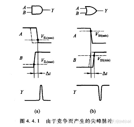
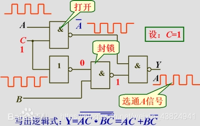
Another important thing is competition and risk. Competition refers to the fact that two input signals jump in opposite directions at the same time. Risk is the phenomenon of unexpected actions in the circuit. It can be said that competition and risk are not necessarily related! Some students may think that competition is a sufficient condition for risk, but in fact competition does not necessarily cause risk, and some students think that competition is a necessary condition for risk, but it is not! The actual engineering situation is very complicated. Even if there is a risky phenomenon, it cannot be said that it must be caused by competition. This is the difference between engineering and theory!
The easiest way to judge competition is to see if there is an AND or OR operation between a certain variable and its own inverse variable in the expression. The solution is to introduce redundant items or add capacitors, but in engineering, this will undoubtedly sacrifice the operating speed of the digital circuit, which is intolerable. So we actually take in more projects in gated approach.
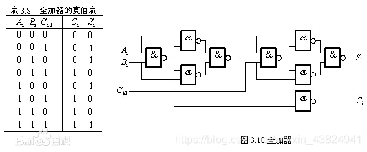
2. Basic Synchronous Sequential Circuits
The basis of sequential circuits is the knowledge of flip-flops, as well as the Boolean algebra used in digital circuits.
The flip-flop and one-time conversion phenomenon should be paid attention to here for the flip-flop. Another thing is that different flip-flops can be converted to each other to meet the actual engineering requirements. This is the same as the conversion of the combinatorial logic function expression mentioned earlier. of.
It should also be mentioned here that the dynamic characteristics of triggers have been weakened in the teaching of many universities in our country, and when I was watching the UCSD tutorials, I found that they paid great attention to dynamic characteristics, including setup time, hold time, transmission delay, etc., will be strictly Calculated and expressed in the sequence diagram, I think this is very worthy of our reference.
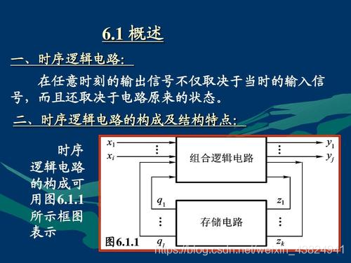
Compared with the combinational logic circuit, the sequential circuit has more storage functions. The combinational logic circuit composed of basic flip-flops can actually store one bit of information, and the initial state strictly determines the secondary state.
Synchronization and asynchrony are important concepts. Synchronization means that the state of all flip-flops is flipped with the same clock. Asynchronous means multiple clocks or does not change with the clock at all (for example, in some chips, the asynchronous setting of 0 can be cleared at any time)
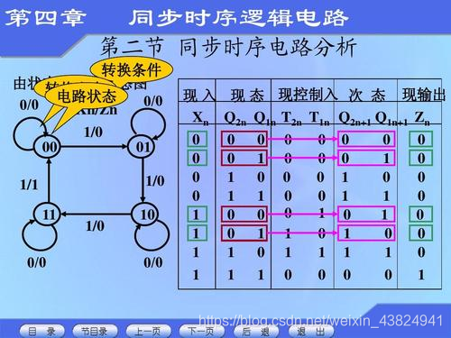
The analysis steps of the synchronous sequential circuit are:
1. Write the clock equation, drive equation and output equation of the circuit according to the circuit diagram
2. The drive equation is brought into the characteristic equation of the flip-flop, and the state equation of each flip-flop is obtained
. 3. According to the clock from the initial state Start to bring in, move step by step
4. Draw the state transition diagram
5. According to the state transition diagram
, the timing diagram 6. Analyze the function, check the self-start
The analysis of the asynchronous sequential circuit mainly pays attention to the different clocks.
The design steps of the synchronous sequential circuit are as follows:
1. Abstract the input variables and output variables according to the actual problem, and determine the number of states (this is very important)
2. Determine the type and number of flip-flops, assuming that the number of flip-flops is n, ensure 2^n>The number of circuit states
3. Draw the Karnaugh map of the secondary state according to the secondary state and the initial state, decompose it if necessary, and then get the state equation
4. The state equation and the trigger characteristic equation are compared to determine the circuit structure
5. Check auto-start and invalid status
This is the end of this issue, thank you for watching!