Study notes (3): Verilog digital logic circuit design method
1. Verilog language design ideas and synthesizable features
Example: Design a modulo 256 (8bits) counter with Verilog
(a) Synthesizable program description method

(b) Common ways of describing errors

At the same time, Verilog has a variety of circuit description methods, which also determines the diversity of circuit design.
Example: Design a digital multiplexer with Verilog
(a) Code in the form of a truth table

(b) codes in the form of logical expressions

(c) codes in the form of structural descriptions

2. Verilog combinational logic circuit
The characteristic of the combinational circuit is that the steady-state output at any time in the circuit only depends on the input at that time, and has nothing to do with the original state of the circuit.
The design of combinational circuits needs to consider the following aspects:
- The number of logic devices used is the least, the types of devices are the least, and the connection between devices is the simplest. Such a circuit is called a "minimization" circuit;
- Secondly, in order to meet the speed requirements, the number of stages should be as small as possible to reduce the delay of the gate circuit; the power consumption of the circuit should be as small as possible, and the work is stable and reliable.
There are four ways to describe combinational logic circuits: structural description, logic algebra, truth table, and abstract description.
For example: Design a voting circuit for 3 referees, when two or more referees agree, the judge will output "1", otherwise it will output "0".
Method 1: The truth table method
The truth table is the most direct and simple way to describe the circuit function. According to the function of the circuit, the logical relationship between the output and the input can be directly established through the truth table. This example has three inputs A, B, C and one output OUT.
| A | B | C | OUT |
|---|---|---|---|
| 0 | 0 | 0 | 0 |
| 0 | 0 | 1 | 0 |
| 0 | 1 | 0 | 0 |
| 1 | 0 | 0 | 0 |
| 0 | 1 | 1 | 1 |
| 1 | 0 | 1 | 1 |
| 1 | 1 | 0 | 1 |
| 1 | 1 | 1 | 1 |
In Verilog, you can use the "case" statement to descriptively design the circuit, design according to the above table:


Method 2: Logic Algebra
Another expression method for combinational circuits is the logic algebra method. The main idea is to express the truth table with a Karnaugh map, and then simplify the circuit to obtain the expression of the logic function.
Through the simplification of the Karnaugh map, the logic function expression between the logic output and input of the combinational circuit can be obtained:

according to the logic function expression, it is very convenient to write Verilog using the logic algebra description method:
module desingn(OUT,A,B,C);
output OUT;
input A,B,C;

assign OUT = (A&B) | (B&C) | (A&C);

endmodule
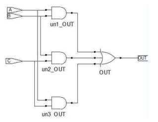
Method 3: Structural description method
The structural description method is the most direct representation of the circuit, and the schematic diagram design usually used in early digital circuit design is actually a structural description method.
module desingn(OUT,A,B,C):
output OUT;
input A,B,C;

and U1(w1,A,B);
and U2(w2,B,C);
and U3(w3,A,C);
or U4(OUT,w1,w2,w3);

endmodule
Method 4: Abstract description method
Verilog also provides a method of circuit design using abstract description, which can directly start from the circuit function and write code. For example, in the design of the decision device, the judgments of the three inputs are added, and when the judgment is successful, the sum of the adder is greater than 1, which means that the voting is successful.
module  desingn(OUT,A,B,C);
output OUT;
input A,B,C;
wire [1:0} sum;
reg OUT;

assign sum = A + B + C;
always@(sum)
	if(sum > 1)
		OUT = 1;
	else
		OUT = 0;
endmodule
2.1 Digital adder
Digital adder is the most commonly used digital operation logic, which is widely used in computer, communication and multimedia digital integrated circuits.
For example: 2-input 1bit signal full adder. Considering the carry from the lower bit, the operation is a full-add operation, and the circuit that realizes the full-add operation is called a full adder.

The algebraic logic is expressed as:

the corresponding circuit is as follows:

Verilog can write a one-bit full adder in different description ways, and its integrated circuit is the same, but the description style is different.
(1) Realized by continuous assignment statement
module one_bit_fulladder(SUM, C_OUT, A, B, C_IN);
input A, B, C_IN;
output Sum, C_OUT;
	assign SUM = (A ^ B) ^ C_IN;
	assign C_OUT = (A & B) | ((A ^ B) & C_IN);
endmodule
(2) Realize by using behavioral description
module one_bit_fulladder(SUM, C_OUT, A, B, C_IN);
input A, B, C_IN;
output SUM, C_OUT;
	assign {C_OUT,SUM} = A + B + C_IN;
endmodule
Using behavioral description can improve the design efficiency. For the behavioral description design of a typical multi-bit adder, it is only necessary to change the bit width of the input and output signals in the code. For example, a 2-input 8bits adder: Example: 4-bit

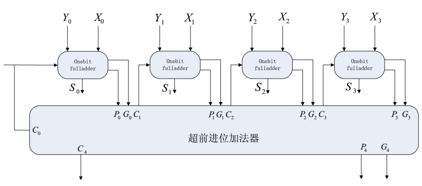
super Carry-forward adder The
carry-forward adder is a high-speed adder. Each stage of carry is generated by an additional combinational circuit. The high-order operation does not need to wait for the completion of the low-order operation, so the operation speed can be improved.
According to the full adder whose input signal bit width is N, its carry signal is:

the output addition result is

The advanced carry flag signal is

The carry generation function is

The carry transfer function is

In the above formula, N is the number of adders, and in a 4-bit adder, N=4. From the formula, the expression of the carry signal at all levels can be deduced, and a fast carry logic circuit can be formed.

The circuit diagram of the 4-bit carry-ahead adder is as follows
: Verilog code of the 4-bit carry-ahead adder:
2.2 Data Comparator
The data comparator is a logic circuit used to compare the size of two binary numbers, or to detect whether they are equal. The data comparator consists of two parts: one is to compare the size of two numbers; the other is to detect whether the two numbers are consistent.
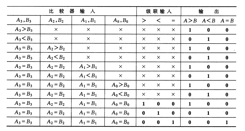
Example: 4-bit numerical comparator
The comparison process of a multi-digit numerical comparator is to compare the high bit to the low bit one by one, and only when the high bit is equal, the low bit is compared. When comparing A 3 A 2 A 1 A 0 and B 3 B 2 B 1 B 0 in a 4-bit numerical comparator , the highest bit A 3 and B 3 should be compared first . If A 3 >B 3 , no matter what the other digits are, the result is A>B; if A 3 <B 3 , A< B. If A 3 =B 3 , it is necessary to judge the size of A and B by comparing the lower bit A 2 and B 2 . If A 2 =B 2 , you must also compare the lower bit of A 1 with B1 to judge until the last bit of comparison. If exactly equal, it is determined by the previous stage result C (cascade input).
module four_bits_comp(F, A, B,C);
parameter comp_width = 4;
output [2:0] F;
input [comp_width-1:0] A;
input [comp_width-1:0] B;
ref [2:0] F;
always@(A or B or C)
	if(A>B)
		F = 3'b100;
	else if(A<B)
		F = 3'b001;
	else
		F = C;
endmodule
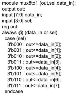
2.3 Data Selector
The data selector is also called a multiplexer (MUX for short), which has n-bit address input, 2 n- bit data input, and 1-bit data output. Each time under the control of the input address, one output is selected from multiple input data, and its function is similar to a single-pole multi-throw switch, as shown in the figure: For example,

8-to-1 data selector
8-to-1 data selector can be composed of multiple 2-to-1 selector composition:

(1) Structure-level description of multiple 2-to-1 data selectors
module mux8to1(d_out, d_in, sel);
output	d_out;
input[7:0] d_in;
input [2:0] sel;
wire[3:0] w1;
wire[1:0] w2;
	assign w1 = sel[0] ? {d_in[7], d_in[5], d_in[3], d_in[1]} : {d_in[6], d_in[4], d_in[2], d_in[0]};
	assign w2 = sel[1] ? {w1[3], w1[1]} : {w1[2], w1[0]};
	assign d_out = sel[2] ? w2[1] : w2[0];
endmodule
(2) Abstract description method
For the design of the multiplexer, it can be designed through the "case" statement.
2.4 Digital Encoder
The process of representing a specific object with words, symbols or numbers is called encoding. Representing related signals in binary codes in digital circuits is called binary coding. The circuit that realizes the encoding operation is called an encoder.
Example: 3-bit binary 8-3-wire encoder A circuit
that uses n-bit binary codes to encode N=2 n general signals is called a binary encoder.
For example, n=3, 8 general signals can be encoded. This encoder has a feature: only one valid signal is allowed to be input at any time, and two or more valid signals are not allowed to appear at the same time.
The following block diagram:

truth table:

module 8to3(F, I);
output [2:0] F;
input [7:0} I;
reg [2:0] F;
always@(I)
	case(I):
		8'b00000001:F=3'b000;
		8'b00000010:F=3'b001;
		8'b00000100:F=3'b010;
		8'b00001000:F=3'b011;
		8'b00010000:F=3'b100;
		8'b00100000:F=3'b101;
		8'b01000000:F=3'b110;
		8'b10000000:F=3'b111;
		 default: F= 3'bx;
	endcase
endmodule
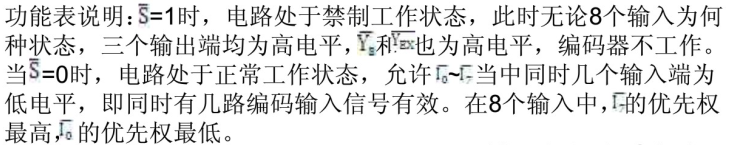
Example: 8-wire-3-wire priority encoder
binary encoder circuit requires only one input to be valid at any time, if two or more input signals are valid at the same time, it will cause output chaos, so there are certain limitations in the use process sex. To overcome the requirement on the input signal, one approach is to use a priority encoder. The priority encoder allows multiple input signals to be effective at the same time, but it only encodes the effective input signal with the highest priority among them, and ignores the input signals with lower levels.
Function table:


example: binary conversion decimal 8421 BCD encoder
The circuit that encodes ten signals such as decimal numbers 0, 1, 2, 3, 4, 5, 6, 7, 8, 9 into binary code is called a binary conversion decimal encoder . Its input is the state information representing the 10 numbers of 0-9, the effective signal is 1 (that is, when a certain signal is 1, it means that it needs to be encoded), and the output is the corresponding BCD code, so it is also called 10-line one 4-wire encoder. It has the same characteristics as the binary encoder, allowing only one valid signal to be input at any time.


Example: The 8421BCD decimal remainder 3 encoder
is the same as the 8421BCD code, the remainder 3 code is also a kind of BCD code, the characteristic of this encoding is that when the remainder 3 code is used for decimal addition, if the sum of the 2 numbers is 10, it is exactly equal to 16 of the binary number, then the carry signal is automatically generated from the high bit, so the remaining 3 codes can be used.
Code table for the remaining 3 yards:


2.5 Digital Decoder
Decoding is the reverse process of encoding, which translates the information represented by the binary code into the corresponding state information. The circuit that realizes the decoding function becomes a decoder.
The figure shows the logic circuit and logic symbols of the 2-4-wire decoder. In the figure, A 1 and A 0 are address input terminals, and A 1 is a high bit. Non-Y 0 - non-Y 3 are status signal output terminals, "not" means that the low point is active. E is the enabling terminal (or gate control terminal), which is active at low level. When E = 0, the decoder is allowed to work, and only one of non-Y 0 - non-Y 3 is allowed to be an active level output; when E = 1, the decoder is prohibited from working, and all outputs are high.
Generally, the enabling terminal has two purposes: one is to introduce a strobe pulse to suppress the occurrence of dangerous pulses; the other is to expand the number of input variables (function expansion).


2.6 Parity Checker
The function of the parity checker is to detect whether the number of "1" in the data is odd or even. In computers and some digital communication systems, parity checkers are commonly used to check data transmissions and digital records for errors.
There are two types of parity: odd and even. Odd parity ensures that the total number of "1" in the transmitted data and parity bits is an odd number. If the data contains an odd number of "1", the check position is "0", and if the data contains an even number of "1", the check position is "1". Even parity ensures that the total number of "1" in the transmitted data and parity bits is an even number. If the data contains an odd number of "1", check the position "1", if the data contains an even number of "1", then check the position "0".
The parity check can only detect some transmission errors, it cannot determine which bit or bits the error occurred in, so it cannot perform error correction. Data can only be resent when an error occurs in the data.
Example: 8bits parity checker
The schematic diagram of the 8bits parity checker is shown in the figure: In the figure, the input b 0 - b 7

of the checker is composed of 7bits data and 1 bit check bit. F OD is the odd output, and F EV is the even output. When using odd parity, F OD = 1, F EV = 0; when using even parity, F OD =0, F EV = 1.


3. Sequential circuit
Unlike combinational logic circuits, the output of sequential logic circuits is not only related to the value of the input variable at the current moment, but also related to the original state of the circuit, that is, the past input conditions.

Sequential logic circuit has two characteristics:
(1) Sequential logic circuit includes two parts: combinational logic circuit and storage circuit. The storage circuit has a memory function and is usually composed of flip-flops; (2)
The state of the storage circuit is fed back to the input terminal of the combinational logic circuit. , together with external input signals determine the output of the combinational logic circuit.
Synchronous sequential circuit design process:

Example: use verilog to design a "111" sequence detector. When three or more "1" are input, the circuit output is 1, otherwise it is 0.
(1) State transition diagram method

S 0 : initial state, indicating that the circuit has not received a valid 1 yet.
S 1 : Indicates that the circuit received a 1.
S 2 : Indicates that the circuit has received two consecutive 1s.
S 3 : Indicates that the circuit has received three consecutive 1s.
Circuit diagram:
module check(z, x, clk);
parameter s0 = 2'b00, s1 = 2'b01, s2 = 2'b10, s3 = 2'b11;
output z;
input x, clk;
reg[1:0} state, next_state;
reg z;
always@(posedge clk)
case(state)
	s0:if(x)
			begin
				next_state <= s1;
				z = 0;
			end
		else
			begin
				next_state <= s0;
				z = 0;
			end
	s1:if(x)
			begin
				next_state <= s2;
				z = 0;
			end
		else
			begin
				next_state <= s0;
				z = 0;
			end
	s2:if(x)
			begin
				next_state <= s3;
				z = 1;
			end
		else
			begin
				next_state <= s0;
				z = 0;
			end
	s0:if(x)
			begin
				next_state <= s3;
				z = 0;
			end
		else
			begin
				next_state <= s0;
				z = 0;
			end
endcase
always@(posedge clk)
	state <= next_state;
endmodule
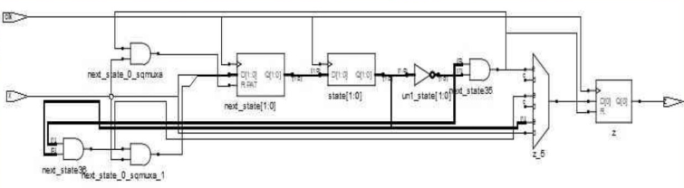
(2) Structural description method based on state simplification
To simplify the state transition diagram, there are only three states left, and two bits of binary representation are required, that is, two D flip-flops are required to store the state. Let Q 1 represent the output of the high register and Q 0 represent the output of the low register. The state jump and output Z are shown in the form of a Karnaugh diagram, as follows: The  output equation and state equation of the circuit can be obtained from the Karnaugh diagram:
Q1n+1 = Q1
Q0n+1 = X
Z = Q1Q0X
//D触发器模块
module DFF(Q, D, clk);
output Q;
input D, clk;
reg Q;
always@(posedge clk)
	Q <= D;
endmodule

//序列检测模块
module check(z, x, clk);
output z;
input x,clk;
wire w1,w2;
DFF U1(.clk(clk), .D(x), .Q(w1));
DFF U2(.clk(clk), .D(w1), .Q(w2));
assign z = x&w1&w2;
endmodule

(3) Verilog HDL abstract description method
In Verilog, the circuit can also be described abstractly. To realize the detection of the sequence "111", a three-bit shift register can be used, and the output x is used as the output of the shift register. When the register is 111, the output Z is 1.
module check(z, x, clk);
output z;
input x,clk;
reg[2:0] q;
reg z;
always@(posedge clk)
	q <= {q[1:0], x};
always@(posedge clk)
	if(q == 3'b111)
		z = 1;
	else
		z = 0;
endmodule

3.1 Triggers
Flip-flops are the most basic circuit units of sequential circuits, mainly including D flip-flops, JK flip-flops, T flip-flops, and RS flip-flops. According to different functional requirements, flip-flops also have functions such as setting, resetting, enabling, and selecting.
3.1.1 Simple D flip-flop

| clk | D | Qn | Qn+1 |
|---|---|---|---|
| 0 | x | 0 | 0 |
| 0 | x | 1 | 1 |
| 1 | x | 0 | 0 |
| 1 | x | 1 | 1 |
| ↑ | 0 | 0 | 0 |
| ↑ | 0 | 1 | 0 |
| ↑ | 1 | 0 | 1 |
| ↑ | 1 | 1 | 1 |
module DFF(Q, D, clk);
output Q;
input D, clk;
reg Q;
always@(posedge clk)
	Q <= D;
endmodule
The data D at the input end is sent to the flip-flop at the rising edge of the clock clk, so that Q=D. Its characteristic equation can be described as Q n+1 = D n .
3.1.2 D flip-flop with reset terminal (clear terminal):

Synchronous clear trigger:
module DFF_rst(q, clk, rst_n, d);
output q;
input clk,rst_n,d;
reg q;
always@(posedge clk)
	if(!rst_n)
		q<=0;
	else
		q<=d;
endmodule
Trigger cleared asynchronously:
module DFF_rst(q, clk, rst_n, d);
output q;
input clk,srst_n,d;
reg q;
always@(posedge clk or rst_n)
	if(!rst_n)
		q<=0;
	else
		q<=d;
endmodule
3.1.3 Complex function D flip-flop
Synchronous clear 0, set 1 and asynchronous clear 0, set 1 complex D flip-flop in one flip-flop.
module DFF(q, qb, clk, rst_n1, set1, rst_n2, set2, data_in);
output q, qb;
input clk, rst_n1,rst_n2, set1,set2, data_in;
reg q,qb;
always@(posedge clk)
	if(!rst_n1)
		q<=0;
	else
		q<=data_in;
always@(posedge clk or rst_n2)
	if(!rst_n2)
		q<=0;
	else
		q<=data_in;
endmodule
3.1.4 T flip-flop
The logic symbol of the T flip-flop is as follows. The function of the T flip-flop: When the effective edge of the clock arrives, if T=1, the flip-flop flips; if T=0, the state of the flip-flop remains unchanged. R is the reset terminal, asynchronous reset, active low.

module TFF(d, t, clk, rst_n);
output d;
input t, clk, rst_n;
reg d;
always@(posedge clk or rst_n)
	if(!rst_n)
		d <= 1'b0;
	else if(t)
		d <= ~d;
endmodule
3.2 Counter
3.2.1 Binary counter

module comp2(q, clk, rst);
output q;
input clk,rst;
reg q;
always@(posedge clk or rst_n)
 if(!rst)
 	q <= 1'b0;
 else
  q <= ~q;
endmodule
3.2.2 Counter with any modulus
For a counter with any modulus value M, the first step is to determine the number of flip-flops required by the counter. N flip-flops correspond to 2 N states. There should be 2 N > M arbitrary modulus counters to select the minimum N that satisfies the conditions, and N is the number of flip-flops in the counter. There are two ways to realize: Feedback clearing method and feedback setting method.
//反馈清零法设计的模11计数器
module comp11(count, clk, rst);
output[3:0] count;
input clk,rst;
reg[3:0] count;
always@(posedge clk)
if(rst)
	count <= 4'b0000;
else
	if(count == 4'b1010)
		count <= 4'b0000;
	else
	 count <= count + 1;
endmodule
3.3 Shift Register
The shift register can be used to realize serial-to-parallel conversion of data, and can also form a shift line counter for counting and frequency division. It can also form a sequence code generator, sequence code detector, etc. It is also widely used in digital systems. One of the sequential logic components.
Example: Ring shift register
N-bit ring register is composed of N shift registers, which can realize ring shift

Use the output of each register as input to the next bit register, and the output of the higher bit register as input to the loop.
module shiftregist(D, clk, rst_n);
parameter shiftregist_width = 4;
output [shiftregist_width-1:0] D;
input clk,rst_n;
reg [shiftregist_width-1:0] D;

always@(posedge clk)
	if(!rst_n)
		D<=4'b0000;
	else
		D<={D[shiftregist_width-2:0], D[shiftregist_width-2:1]};
endmodule
3.4 Sequence Signal Generator
Sequence signals are commonly used functional units in digital circuit systems. According to the relationship between the sequence cycle length M and the number of flip-flops n, they can generally be divided into three types: (1) The
maximum cycle length sequence code, M=2 n ;
(2) The longest line Shape sequence code (m sequence code), M=2 n -1;
(3) Arbitrary cyclic length sequence code, M<2 n .
A sequence signal generator is a sequential circuit that can generate one or more sets of sequence signals. It can be composed of a pure sequential circuit or a hybrid circuit including sequential and combinational logic.
Example: Design a signal generator that generates a sequence of 10011
- Method (1): Composed of a shift register
Since there is no combination circuit between the input and output signals of the shift register, and no feedback operation through combination logic is required, the operating frequency of this sequence generation circuit is very high. The disadvantage is that the length of the shift register depends on the length of the sequence, so it occupies a large area of the circuit.
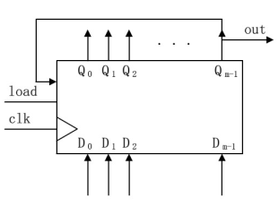
module maker(out, clk, load, D);
parameter M=6;
output out;
input clk,load;
input [M-1:0] D;
reg [M-1:0] Q;
initial Q=6'b10011;
always@(posedge clk)
	if(load)
		Q<=D;
	else
		Q<={Q[M-2:0], Q[M-1]};
assign out=Q[M];
endmodule
Method (2): The structural block diagram of the feedback shift sequence code generator composed of a shift register and a combinational logic circuit is shown in the figure. It is composed of a shift register and a combinational logic network. A periodic sequence code can be obtained.

Its design is carried out according to the following steps:
(1) According to the cycle period M of the given sequence signal, determine the number of bits n of the shift register, 2 n-1 < M ≤ 2 n .
(2) Determine M independent states of the shift register. According to the shift rule, the given sequence code is divided into M states every n bits. If repetition occurs in M states, the number of bits in the shift register should be increased. Repeat the above process with n+1 bits until it is divided into M independent states.
(3) List the state sequence table and feedback function table of the shift register according to M different states, and find the expression of the feedback function F.
(4) Check the self-starting performance.
Compared with the sequence signal generator above, the output of each register needs to pass through the feedback network before being connected to the input of the shift register. Therefore, the speed of the circuit will inevitably decrease, but the benefit of the feedback network is that it can save registers.
Signal generator for the "1001 1 1" sequence.
First, determine the number n of shift registers required. Since M = 6, n is 3.
Then, six independent states of the shift register are determined.
According to the law, every group of three digits is divided into six states as 100,001,011,111,111,110. The state 111 appears repeatedly, so n=4 is taken, and the state is re-divided to obtain: 1001, 0011, 0111, 1111, 1110, 1100. Therefore, n=4 is determined.
Thirdly, list the state sequence table and the feedback excitation function table, and find the expression of the feedback function F.
First list the state sequence table, and then list the feedback excitation function table according to the shift input required by each state, that is, the feedback input signal, as shown in the following table. Find the feedback activation function:


//反馈移位型序列信号发生器
module maker(out, clk, load, D);
parameter M=4;
output out;
input clk,load;
input [M-1:0] D;
reg {M-1:0] Q;
wire w1;

always@(posedge clk)
	if(load)
		Q<=D;
	else
		Q<={Q[M-2:0],ww1};
	assign w1 = (~Q[3])|((~Q[1])&(~Q[0]))|(Q[3]&(~Q[2]));
	assign out =Q[M-1];
endmodule
Method (3): Composed of counters
The counting sequence signal generator and the feedback sequence signal generator are roughly the same, and they are both composed of a sequential circuit and a combinational circuit. The difference is that the timing state of the feedback sequence signal generator is generated by the shift register, and the output takes the highest bit of the register; while in the counting type sequence signal generator, the counter is used instead of the shift register to generate the timing state, and the output is generated by the combinational circuit .
The advantage of the counting type is that the state setting of the counter is not directly related to the output sequence, and there is no need to determine the state according to the output as above. You only need to design the feedback network well. Therefore, the counting structure is more convenient for changing the output sequence, and as long as it is connected to different feedback networks, it can generate multiple sets of sequence codes at the same time.

The design process is divided into two steps:
first, design the modulo M counter according to the length M of the sequence code, and the state can be customized;
second, design the combined output network according to the state transition relationship of the counter and the requirements of the sequence code. Signal generator for the "100111" sequence. The M value of the sequence signal is 6, because a modulo 6 counter needs to be selected. The state selection of the counter is from 000 to 101, and the following table can be obtained.

The Karnaugh map can be drawn from the truth table to obtain the output function:

the following code:
module maker(OUT, clk, reset);
parameter M=3;
input clk,reset;
reg [M-1:0] counter;
always@(posedge clk)
	if(!reset)
		counter <= 3'b000;
	else
		counter <= counter + 1;
	assign OUT = counter[2] | ((~counter[1])&(~counter[0])) | (counter[1]&counter[0]);
endmodule
Example: Designing a pseudo-random code generator
Random code is a binary code whose change rule is similar to that of random code. It can be used as a signal source in digital communication and sent to the receiver through a channel to detect the probability of error code in digital communication system. , that is, the bit error rate.
In traditional digital circuit design, the pseudo-random sequence signal generator is realized by a shift-storage counter, and the input signal of the feedback network is taken from part of the output terminals (Q N-1 ~ Q 0 ) of the shift register , which The output F of the feedback to the serial input of the shift register.
Through different feedback networks, different transfer-type counters can be formed. Taking the m-sequence code as an example, the feedback function is shown in the following table, where N in the table is the number of flip-flops, and F is the list of feedback functions.

For example, N = 4, the feedback function is as follows:

Take N = 4 as an example, in the 15-bit longest linear sequence shift counter, there is an infinite loop composed of "0000", in order to break the infinite loop, the formula can be modified as :

shift register counter according to the longest linear sequence of N=4:
module signal(out, clk, load_n, D_load);
output out;
input load_n,clk;
input [3:0] D_load;
reg [3:0] Q;
wire F;
always@(posedge clk)
	if(~load_n)
		Q<=D_load;
	else
		Q<={Q[2:0],F};
	assign F = (Q[1]^Q[0]) | (~Q[3]&~Q[2]&~Q[1]&~Q[0]);
	assign out = Q[3];
endmodule
4. Finite Synchronous State Machine
The finite state machine is a general model of sequential circuits, and any sequential circuit can be expressed as a finite state machine. The finite state machine is essentially a sequential circuit composed of registers and combinational logic. The transition between states is always triggered by the clock, and the state information is stored in the register. It is called because the number of states is finite 有限状态机.
Like other sequential circuits, the finite state machine is also composed of two parts: storage circuit and combinational logic circuit. The storage circuit is used to generate the state of the state machine; the combinational logic circuit is used to provide the output and the conditions for the state machine to jump.

According to the way the output signal is generated, the finite state machine can be divided into two types: Mealy type and Moore type. The output of the Mealy-type state machine is related to the current state and input, while the output of the Moore-type state machine only depends on the current state and has nothing to do with the input.

There are many encoding methods for state machines, and the resulting circuits are also different. There are three common encoding methods: binary encoding, gray encoding, and one-bit one-hot encoding.
(1) Binary coding: The status register is composed of flip-flops. N flip-flops can form 2 n states. The advantage of binary coding is that it uses fewer flip-flops and saves resources; the disadvantage is that multiple bits may change at the same time when the state jumps, causing glitches and logic errors.
(2) Gray coding: Gray coding is similar to binary coding. Only one bit changes when the Gray coding state jumps, which reduces the possibility of glitches and some transient states.
(3) One hot encoding: n bits are used to encode n states, and only one bit in each state encoding is 1, such as: 0001, 0010, 0100, 1000. One hot encoding increases the number of flip-flops used, but this encoding is convenient for decoding and can effectively save and simplify combinational circuits.
In Verilog, there are many ways to write finite state machines, two-stage and three-stage are commonly used.
(1) Two-stage description of the state machine:
//第一个进程,同步时序always模块,格式化描述次态寄存器迁移到现态寄存器
always@(posedge clk or negedge rst_n) //异步复位
	if(!rst_n)
		current_state <= IDLE;
	else
		current_state <= next_state; //注意,使用的是非阻塞赋值
	//第二个进程,组合逻辑always模块,描述状态转移条件判断
always@(current_state) //电平触发
	begin
		next state = x; //要初始化,使得系统复位后能进入正确的状态
		case(current_state)
			S1:if(...)
				next_state=S2; //阻塞赋值
				out1<= 1'b1;//注意是非阻塞逻辑
				...
		endcase
	end
(2) Three-stage description of the state machine:
//第一个进程,同步时序always模块,格式化描述次态寄存器迁移到现态寄存器
always @ (posedge clk or negedge rst_n) //异步复位
	if(!rst_n)
		current_state <= IDLE;
	else
		current_state <= next_state;//注意,使用的是非阻塞赋值
//二个进程,组合逻辑always模块,描述状态转移条件判断
always @ (current_state) //电平触发
	begin
		next_state=x; //要初始化,使得系统复位后能进入正确的状态
		case(current_state)
		S1:if(...)
			next_state=S2; //阻塞赋值
			...
		endcase
	end
//第三个进程,同步时序always模块,格式化描述次态寄存器输出
always@(posedge clk or negedge rst_n)
...//初始化
case(next_state)
	S1:
		out1 <= 1'b1;//注意是非阻塞逻辑
	S2:
		out2 <= 1'b1;
	default:... //default的作用是免除综合工具综合出锁存器。
endcase
end
//三段式不一定要写三个always块,如果状态机更为复杂,always块也会相应增加。
Example: Designing a sequential pulse generator
A sequential pulse generator is also called a pulse distributor, which distributes high-level pulses to different outputs in sequence. It is guaranteed that only one output is a high-level pulse in each clock, and the pulse levels on different clocks appear in all outputs in sequence.
Take the 4-bit sequential pulse generator as an example, it has four outputs W 0 W 1 W 2 W 3 , high-level pulses appear in sequence on each output, and the output cycles between 1000, 0100, 0010, and 0001. State transition diagram of the 4-bit sequential pulse generator. As shown in the figure, it consists of 4 states, and the number of "1" in each state is 1, which means that only one output terminal is high level (pulse) in each clock cycle, and it appears in turn, so the generated sequential pulse signal.

When encoding a four-state machine, only two bits of binary encoding are required:
module state4(out, clk);
output [3:0] out;
input clk;
reg [3:0] out;
reg [1:0] state, next_state;
always@(state)
	case(state)
		2'b00:
			begin
				out <= 4'b1000;
				next_state <= 2'b01;
			end
		2'b01:
			begin
				out <= 4'b0100;
				next_state <= 2'b10;
			end
		2'b10:
			begin
				out <= 4'b0010;
				next_state <= 2'b11;
			end
		2'b00:
			begin
				out <= 4'b0001;
				next_state <= 2'b010;
			end
	endcase
always@(posedge clk)
	state <= next_state;
endmodule
Example: Design a newspaper vending machine, the price of the newspaper is 8 cents, and the banknotes are 1 cent, 2 cents, 5 cents, and one yuan. This newspaper machine does not consider the special circumstances such as the large denomination of coins. The following figure is the state transition diagram of the newspaper machine. In the figure, S0 ~ S7 are the 8 states of the state machine, and the subscripts represent the sum of the coins that have been inserted. For example, SO means that there is no coin, and S1 means that 1 jiao has been invested. analogy. M stands for input, M1 stands for putting in 1 jiao coin, M2 stands for putting in 2 jiao coins, M5 stands for putting in 5 jiao coins, and M10 stands for putting in one yuan.

Verilog code:
//data_out=1表示给出报纸,data_out_return=1表示找回1角硬币,data_out_return2=1表示找回2角硬币
module auto_sellor(current_state,data_out, data_out_return1, data_out_retum2, clk, rst_n, data_in);
parameter state_width = 3, data_in_width = 3;
output [state_width-1:0] current_state;
output data_out, data_out_return1, data_out_return2;
input [data_in_width-1:0] data_in;
input clk, rst_n;
reg [state_width-1 :0] current_state, next_state;
reg data_out, data_out_return1, data_out_return2;
always@(current_state or rst_n)
	if (!rstn)
		next_statec=0;
	else
		case(current_state)
			3'b000:
				case(data_in)
					3'b000:
						begin
							next_state <= 3'b000;
							data_out <=1'b0;
							data_out_return1 <=1'b0;
							data_out_return2 <= 1'b0;
						end
					3'b001:
						begin
							next_state <= 3'b001;
							data_out <=1'b0;
							data_out_return1 <=1'b0;
							data_out_return2 <= 1'b0;
						end
					3'b010:
						begin
							next_state <= 3'b010;
							data_out <=1'b0;
							data_out_return1 <=1'b0;
							data_out_return2 <= 1'b0;
						end
					3'b011:
						begin
							next_state <= 3'b101;
							data_out <=1'b0;
							data_out_return1 <=1'b0;
							data_out_return2 <= 1'b0;
						end
					3'b100:
						begin
							next_state <= 3'b000;
							data_out <=1'b1;
							data_out_return1 <=1'b0;
							data_out_return2 <= 1'b1;
						end
				endcase
			3'b001:
				case(data_in)
					3'b000:
						begin
							next_state <= 3'b001;
							data_out <=1'b0;
							data_out_return1 <=1'b0;
							data_out_return2 <= 1'b0;
						end
					3'b001:
						begin
							next_state <= 3'b010;
							data_out <=1'b0;
							data_out_return1 <=1'b0;
							data_out_return2 <= 1'b0;
						end
					3'b010:
						begin
							next_state <= 3'b011;
							data_out <=1'b0;
							data_out_return1 <=1'b0;
							data_out_return2 <= 1'b0;
						end
					3'b011:
						begin
							next_state <= 3'b110;
							data_out <=1'b0;
							data_out_return1 <=1'b0;
							data_out_return2 <= 1'b0;
						end
				endcase
			3'b010:
				case(data_in)
					3'b000:
						begin
							next_state <= 3'b010;
							data_out <=1'b0;
							data_out_return1 <=1'b0;
							data_out_return2 <= 1'b0;
						end
					3'b001:
						begin
							next_state <= 3'b011;
							data_out <=1'b0;
							data_out_return1 <=1'b0;
							data_out_return2 <= 1'b0;
						end
					3'b010:
						begin
							next_state <= 3'b100;
							data_out <=1'b0;
							data_out_return1 <=1'b0;
							data_out_return2 <= 1'b0;
						end
					3'b011:
						begin
							next_state <= 3'b111;
							data_out <=1'b0;
							data_out_return1 <=1'b0;
							data_out_return2 <= 1'b0;
						end
				endcase
			3'b011:
				case(data_in)
					3'b000:
						begin
							next_state <= 3'b011;
							data_out <=1'b0;
							data_out_return1 <=1'b0;
							data_out_return2 <= 1'b0;
						end
					3'b001:
						begin
							next_state <= 3'b100;
							data_out <=1'b0;
							data_out_return1 <=1'b0;
							data_out_return2 <= 1'b0;
						end
					3'b010:
						begin
							next_state <= 3'b101;
							data_out <=1'b0;
							data_out_return1 <=1'b0;
							data_out_return2 <= 1'b0;
						end
					3'b011:
						begin
							next_state <= 3'b000;
							data_out <=1'b1;
							data_out_return1 <=1'b0;
							data_out_return2 <= 1'b0;
						end
				endcase
			3'b100:
				case(data_in)
					3'b000:
						begin
							next_state <= 3'b000;
							data_out <=1'b0;
							data_out_return1 <=1'b0;
							data_out_return2 <= 1'b0;
						end
					3'b001:
						begin
							next_state <= 3'b101;
							data_out <=1'b0;
							data_out_return1 <=1'b0;
							data_out_return2 <= 1'b0;
						end
					3'b010:
						begin
							next_state <= 3'b110;
							data_out <=1'b0;
							data_out_return1 <=1'b0;
							data_out_return2 <= 1'b0;
						end
					3'b011:
						begin
							next_state <= 3'b000;
							data_out <=1'b0;
							data_out_return1 <=1'b0;
							data_out_return2 <= 1'b0;
						end
				endcase
			3'b101:
				case(data_in)
					3'b000:
						begin
							next_state <= 3'b101;
							data_out <=1'b0;
							data_out_return1 <=1'b0;
							data_out_return2 <= 1'b0;
						end
					3'b001:
						begin
							next_state <= 3'b110;
							data_out <=1'b0;
							data_out_return1 <=1'b0;
							data_out_return2 <= 1'b0;
						end
					3'b111:
						begin
							next_state <= 3'b011;
							data_out <=1'b0;
							data_out_return1 <=1'b0;
							data_out_return2 <= 1'b0;
						end
					3'b011:
						begin
							next_state <= 3'b000;
							data_out <=1'b1;
							data_out_return1 <=1'b0;
							data_out_return2 <= 1'b1;
						end
				endcase
			3'b110:
				case(data_in)
					3'b000:
						begin
							next_state <= 3'b110;
							data_out <=1'b0;
							data_out_return1 <=1'b0;
							data_out_return2 <= 1'b0;
						end
					3'b001:
						begin
							next_state <= 3'b111;
							data_out <=1'b0;
							data_out_return1 <=1'b0;
							data_out_return2 <= 1'b0;
						end
					3'b010:
						begin
							next_state <= 3'b000;
							data_out <=1'b1;
							data_out_return1 <=1'b0;
							data_out_return2 <= 1'b0;
						end
				endcase
			3'b111:
				case(data_in)
					3'b000:
						begin
							next_state <= 3'b111;
							data_out <=1'b0;
							data_out_return1 <=1'b0;
							data_out_return2 <= 1'b0;
						end
					3'b001:
						begin
							next_state <= 3'b000;
							data_out <=1'b1;
							data_out_return1 <=1'b0;
							data_out_return2 <= 1'b0;
						end
				endcase
always@(posedge clk ir rst_n)
	if(!rst_n)
		current_state <= 3'b000;
	else
		current_state <= next_state;
endmodule
Example: "11010" sequence detector
The sequence detector is to detect a specified sequence from the digital code stream. When the sequence 11010 appears at the input, the output is 1, otherwise the output is 0. Repeated sequences are not considered here, that is, the sequence detection is restarted after the specified sequence appears, and the previous data is no longer considered. It is stipulated that the data is input from the right end, that is, input in the order of 1-1-0-1-0. The state transition diagram of the sequence detector is as follows:

module seqdet(dout,din,restn,clk);
parameter IDLE = 3'd0, A = 3'd1, B = 3'd3, C = 3'd4, E = 3'd5;
output dout;
input din,rstn,clk;
reg[2:0] state,next_state;
wire dout;
assign dout = (state==E)?1:0;
always@(posedge clk or negedge rstn)
	if(!rstn)
		state = IDLE;
	else
		case(state)
			IDLE:
					if(din)
						next_state = A;
					else
						next_state = IDLE;
			A:
				if(din)
					next_state = B;
				else
					next_state = IDLE;
			B:
				if(din)
					next_state = B;
				else
					next_state = C;
			C:
				if(din)
					next_state = D;
				else
					next_state = IDLE;
			D:
				if(din)
					next_state = B;
				else
					next_state = IDLE;
			E:
				if(din)
					next_state = IDLE;
				else
					next_state = A;
			default:
				next_state = IDLE;
		endcase
always@(posedge clk)
		state <= next_state;
endmodule