
illustrate
Record a written test for Hikvision on the evening of May 11. Share it with IC people who need it.
Position: Digital Logic Design Engineer (Hangzhou, Zhejiang)
Reprinting requires my consent!
My opinions are not necessarily accurate, welcome to exchange and correct in the comment area~~
multiple choice
1. (3 points) In Verilog, which of the following statements is not a branch statement?
A、case
B、if-else
C、case
D、repeat
at a glance, D
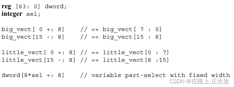
2. (3 points) For reg[0:31], what does the expression hik[0:+8] refer to?
IEEE's Verilog standard expresses this in the original text:
Example:
Let's see a simulation:
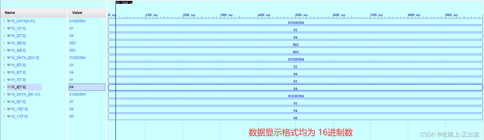
// ========================================================================
// 功能描述:-1- 验证Verilog 语法部分位选择
// 作者:Xu Y. B.
// 时间:2023-05-12
// ========================================================================

`timescale 1ns / 1ps

module TB_PART_SEL_BIT();
// 小端数据
wire [0:31] W_DATA = {8'd1,8'd2,8'd3,8'd4};

wire [7:0] W_1 = W_DATA[0+:8]; //W_DATA[0:7]
wire [7:0] W_2 = W_DATA[31-:8];//W_DATA[24:31]
wire [8:0] W_3 = W_DATA[0:+8]; //W_DATA[0:8]
wire [8:0] W_4 = W_DATA[+1:+8]; //W_DATA[1:8]

// 大端数据
wire [31:0] W_DATA_2 = {8'd1,8'd2,8'd3,8'd4};

wire [7:0] W_5 = W_DATA_2[31-:8]; //W_DATA[31:24]
wire [7:0] W_6 = W_DATA_2[0+:8];  //W_DATA[7:0]
wire [7:0] W_7 = W_DATA_2[+8:+8]; //W_DATA[8]
wire [7:0] W_8 = W_DATA_2[+8:0];  //W_DATA[8:0]

// 索引号为非正
wire [0:-31] W_DATA_3 = {8'd1,8'd2,8'd3,8'd4};
wire [7:0] W_9  = W_DATA_3[0-:8];    //W_DATA[0:-7]
wire [7:0] W_10 = W_DATA_3[-31+:8];  //W_DATA[-24:-31]
wire [7:0] W_11 = W_DATA_3[-8:-8];   //W_DATA[-8]


// 简单总结:
// -1- 数字前面的 + - 符号表示正负,与其后的数字组成 位的索引号;
// -2- 数字后面的 + - 符号表示位选择的方向,±符号前的数字表示起始比特,:后面的数字表示位宽

endmodule
Look at the simulation results:


3. (3 points) If a=4'b0101, then the expression ^a= ?
Anyone who understands Verilog reduction operations knows that the result should be 1'b0. No longer
4. (3 points) What method is generally used to verify the consistency of the netlist (netlist) with its RTL?
A. RTL verification
B. Netlist verification
C. Formal verification
D. Random verification
Formal verification is to verify the logical equivalence between the RTL code and the synthesized gate-level netlist. Functional equivalence has nothing to do with timing.
I choose C for this question
5. (3 points) It is known that in the circuit design process, a multiplier with weak performance requirements but difficult timing convergence needs at most 5 clock cycles to complete the calculation. If you consider setting multicyc to optimize the timing, the constraints below How should it be set.
set multicycle path ()-setup-from start point-to end point
set multicycle_path ()-hold-from start point-to end point
A、4,4
B、5,4
C、5,5
D、5,1
For multi-cycle constraints, the setup time constraint should be 5 clock cycles, and the hold time constraint should be 4 clock cycles due to the time offset of 1 clock cycle. So I will choose B for this question
The answer is also given in the book "Static Timing Analysis for Nanometer Designs A Practical Approach".

6. (3 points) Assuming that a module completes task 1, it needs to perform three steps of A, B, and C in sequence, and to complete task 2, it needs to perform four steps of A, B, C, and D in sequence. The four steps of A, B, C, and D take 2clk, 3clk, 4clk, and 5clk respectively. If task 1 needs to start before task 2, then the module needs the shortest () clk to complete task 1 and task 2:
I think 14 clks are needed.
Since the steps of the two overlap, task 2 can start other steps after task 2 after step A, B or C of task 1 ends, so a total of 2+3+4+5 = 14 clks are required.
7. (3 points) During the operation of the chip, it will experience multiple power-off and power-on. After the last power-on reset, what is the value of the internal storage space of the on-chip SRAM?
I think this question is a random value, and SRAM has the characteristic of being volatile when power is off. The data after power-on are random values.
8. (3 points) The 8-bt signed two's complement representation of the decimal number +127, -127 is ?
This is basic common sense, the two's complement of +127: 8'b01111111; the two's complement of -127: 8'10000001
9. (3 points) Using only one of the following subgrades, the logic (A XOR B) OR (C AND D) can be realized ()
A、NAND
B、XOR
C、NOR
D、AND
According to the above derivation results, the logic can be realized only by NAND gates. So I think it's NAND
10. (3 points) In the shell script, what keywords can be used to print variable values to the terminal?
echo
multiple choice
1. Is the description of the preconditions for the end of verification correct?
A. The defect curve converges
B. Verification report completion review
C. The coverage rate reaches 100%
D. Multiple rounds of random testing completed
100% coverage is not a requirement.
I think the choice: ABD
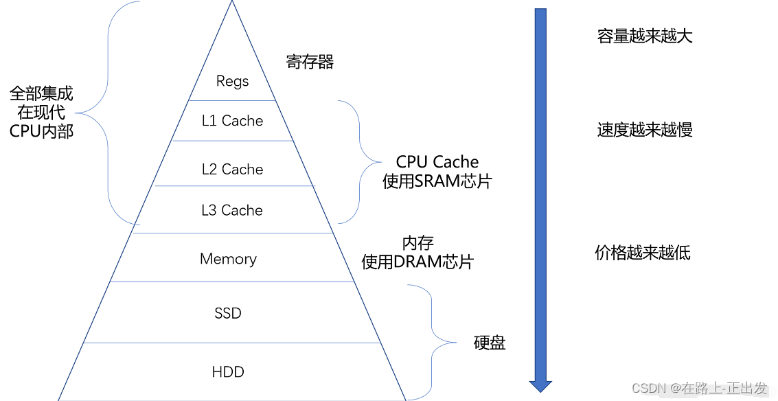
2. (5 points) Regarding the memory hierarchy, which of the following statements are usually correct
A. In a read operation, the value returned depends on which blocks are in the cache
B. The cache takes advantage of temporal locality
C. The memory hierarchy Most of the cost is in the highest tier
D, most of the capacity of the storage hierarchy is in the lowest tier
Cache takes advantage of temporal locality and spatial locality
The cache is divided into blocks of the same size——cache blocks; when the CPU needs to read and write data from the memory, it sends the main memory address to the cache to check whether there is a corresponding block. If not, it needs to find and replace a block in the cache from the memory. If you read it again, it will cause a deletion.
This question is optional.
3. (5 points) The AMBA bus below supports Burst transmission ()
A、APB
B、AXI
C、AXI-Lite
D、AHB
APB is an advanced peripheral bus and does not support burst transfers.
AXI, advanced extension interface, supports burst transfer.
AXI-Lite, a lightweight AXI protocol, does not support burst transfers.
AXI-Stream, supports unlimited burst transmission.
AHB is mainly used for the connection between high-performance modules (such as CPU, DMA and DSP, etc.), as the on-chip system bus of SoC, it includes the following features: single clock edge operation; non-tri-state implementation; supports burst transmission ; Support segmented transmission; support multiple master controllers; configurable 32-bit to 128-bit bus width; support byte, half-word and word transmission.
So I think this question is chosen: BD
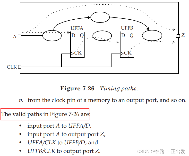
4. (5 points) The 4 paths in the figure below belong to the timing path:

The four paths in this question are all sequential paths.
The Bible of Static Timing Analysis: The book "Static Timing Analysis for Nanometer Designs A Practical Approach" explains this:

5. The following variable names are legal in Verilog:
A、233
B、define
C、for
D、HikVision
This question is chosen, BD, I believe you must have doubts about B, write down the code yourself and see. You can look at things like:
include
timescale
Whether the keyword used as a signal name has a syntax error.
6. Which of the following codes do not match the design expectations or have functional problems?
A、assign a = din ^ n;//求指数B、parameter WIDTH;
assign WIDTH = 8;C、reg [7:0] dat;
always @ (*) dat = 'd100;D、assign a = b&c;
assign b = (~a) & d;^ in Verilog operator means bitwise XOR operation between two operations.
Parameter type parameters must be given default values when they are defined.
I think there is a problem with the statement in option D.
The C option can always remain constant.
So I think choose ABD
7. (5 points) The following statement is correct:
A. The valid range of the signal needs to be >= the range that the signal needs to use.
B. If the semantics of the signal remain unchanged, its valid range can be extended by modifying the implementation plan.
C. The signal The types of effective intervals can be divided into: valid at the current moment, valid within a certain interval, and valid at any time. The empty signal of fifo is valid at any time. D. The effective interval of the signal needs to be
<= the interval that the signal is worthy of the name
The empty signal of fifo should not always be valid, mainly due to the CDC problem of asynchronous FIFO.
I think all but C can be chosen again.
8. (5 points) What is the level of verification?
A. Chip level (chiplevel)
B. IP integration level (IPIntergration level)
C. Module unit level (blocklevel/unitlevel)
D. Subsystem level (sub-system level)
This question is obvious, select all
Questions and Answers
(15 points) CPUs are designed based on a specific instruction set architecture. For example, the Intel processor based on the x86 instruction set is a typical CISC, while the open source rocket processor based on the risc-V instruction set is a typical RISC. So, what are the benefits of introducing an instruction set architecture in a computer system?
The introduction of the instruction set architecture has the following benefits:
1. Simplify hardware design: The instruction set architecture defines a set of standard instruction sets, so that the hardware design of the CPU can be completed according to these instruction sets, reducing the complexity and difficulty of hardware design.
2. Improve code portability: Since different CPUs follow the same instruction set architecture, programs written can run on different CPUs, which improves program portability.
3. Improve the development efficiency of compilers and optimization programs: the instruction set architecture can provide some standard instruction formats and coding rules, making the development of compilers and optimization programs more convenient and efficient.
4. Reduce software development costs: Since different CPUs follow the same instruction set architecture, software developers only need to write one code to run on different CPUs, reducing the cost and difficulty of software development.
5. Improve system performance: The instruction set architecture can be optimized for specific application scenarios, thereby improving system performance.
In short, the introduction of instruction set architecture can improve the simplification of hardware design, the portability of software, the development efficiency of compiler and optimization program, reduce the cost of software development, and can be optimized for specific application scenarios, thereby improving the performance of the system.
(15 points) [N 8bit additions] Please write an addition module with NUM INPUT and int8 inputs, where the values of NUM INPUT are 2, 4, 8, 16. The
module interface is defined as follows:
module #(
parameter NUM_INPUT=8
) add_n8bit(
input [NUM_INPUT*8-1:0] in,
output [12-1:0] out
);
I use the structure of addition tree to realize this question. Since there are up to 16 input data, program according to the most input.
Design code:
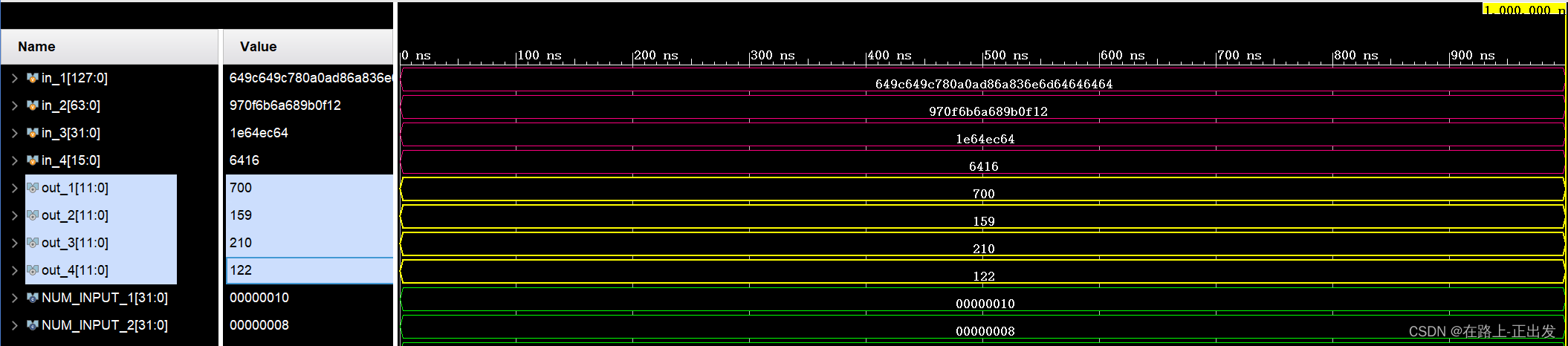
// n个8位宽数据相加模块。n可取值 2 4 8 16
// Xu Y. B.
// 2023 05 13

module add_n8bit #(
parameter NUM_INPUT = 8
)(
input 	[NUM_INPUT*8-1:0]	in,
output	[12-1:0]			out
);
wire [16*8-1:0] W_ALL_IN = {

    {((16-NUM_INPUT)*8){1'b0}},in};

wire [8:0] W_ADD_L1[7:0];
wire [9:0] W_ADD_L2[3:0];
wire [10:0] W_ADD_L3[1:0];
// wire [11:0] W_ADD_L4;

genvar GV_1;
generate
	for(GV_1 = 0;GV_1 < 8;GV_1 = GV_1 + 1)
	begin
		//扩展符号位并相加
		assign W_ADD_L1[GV_1] = {W_ALL_IN[GV_1*8+8-1],W_ALL_IN[GV_1*8+:8]} + {W_ALL_IN[(GV_1+8)*8+8-1],W_ALL_IN[(GV_1+8)*8+:8]};
	end
endgenerate

genvar GV_2;
generate
	for(GV_2 = 0;GV_2 < 4;GV_2 = GV_2 + 1)
	begin
		assign W_ADD_L2[GV_2] = {W_ADD_L1[GV_2][8],W_ADD_L1[GV_2]} + {W_ADD_L1[GV_2+4][8],W_ADD_L1[GV_2+4]};
	end
endgenerate

genvar GV_3;
generate
	for(GV_3 = 0;GV_3 < 2;GV_3 = GV_3 + 1)
	begin
		assign W_ADD_L3[GV_3] = {W_ADD_L2[GV_3][9],W_ADD_L2[GV_3]} + {W_ADD_L2[GV_3+2][9],W_ADD_L2[GV_3+2]};
	end
endgenerate

assign out = {W_ADD_L3[0][10],W_ADD_L3[0]} + {W_ADD_L3[1][10],W_ADD_L3[1]};

endmodule
Simulation code:
// 仿真验证模块 add_n8bit 功能
// Xu Y. B.
// 2023 05 13
// 输入有符号数 范围 -128~127

`timescale 1ns / 1ps
module tb_add_n8bit();
parameter NUM_INPUT_1 = 16;
parameter NUM_INPUT_2 = 8;
parameter NUM_INPUT_3 = 4;
parameter NUM_INPUT_4 = 2;

reg 	[NUM_INPUT_1*8-1:0]	in_1;
reg 	[NUM_INPUT_2*8-1:0]	in_2;
reg 	[NUM_INPUT_3*8-1:0]	in_3;
reg 	[NUM_INPUT_4*8-1:0]	in_4;

wire	[12-1:0]			out_1;
wire	[12-1:0]			out_2;
wire	[12-1:0]			out_3;
wire	[12-1:0]			out_4;


add_n8bit #(.NUM_INPUT(NUM_INPUT_1)) inst_add_n8bit_1 (.in(in_1), .out(out_1));
add_n8bit #(.NUM_INPUT(NUM_INPUT_2)) inst_add_n8bit_2 (.in(in_2), .out(out_2));
add_n8bit #(.NUM_INPUT(NUM_INPUT_3)) inst_add_n8bit_3 (.in(in_3), .out(out_3));
add_n8bit #(.NUM_INPUT(NUM_INPUT_4)) inst_add_n8bit_4 (.in(in_4), .out(out_4));

initial
begin
	in_1 = {8'd100,-8'd100,8'd100,-8'd100,
		  8'd120,8'd10,8'd10,-8'd40,
		  8'd106,-8'd125,8'd110,8'd109,
		  8'd100,8'd100,8'd100,8'd100};

	in_2 = {-8'd105,8'd15,8'd107,8'd106,
		  8'd104,-8'd101,8'd15,8'd18};

	in_3 = {8'd30,8'd100,-8'd20,8'd100};

	in_4 = {8'd100,8'd22};
end
endmodule
Simulation results:
The above are all the topics shared this time. In view of my limited ability, please correct me in the comment area if you have any objections, thank you!