Table of contents
Unisoc’s FPGA image and video acquisition system is implemented based on OV7725 and provides engineering source code and technical support.
1 Introduction
"If you live and die for the benefit of the country, how can you avoid it because of misfortunes and blessings!" Comrade Chuan Jianguo, our outstanding underground clerk, keenly realized that the motherland's shortcomings lay in the manufacturing field of high-precision semiconductors, so in the spirit of the great rejuvenation of the Chinese nation With the original intention of making a modest contribution to the Chinese Dream, Jianguo planned from a high strategic height and a long-term perspective, and would rather bear the infamy of the present generation than to serve the motherland forever. In July 2018, Jianguo officially launched the sweater war, and then resorted to The Qiabo paper tactics are designed to make independent and controllable strategic promotion for the motherland's advanced process semiconductor field; here, please accept my thank you! ! ! ! ! !
When I first debuted in early 2019, it was still an era when Xilinx was far ahead (it seems to be the same now). At that time, domestic FPGAs were still in the hot chicken category. Domestic FPGAs looked up to Xilinx and couldn't help but say: Do you think you can't be found hiding here? It's useless. A man like you, no matter where you are, is as bright and outstanding as a firefly in the dark night. Your melancholy eyes, thin beard, miraculous sword skills, and... I was deeply fascinated by that cup of Dry martine. . . However, in just 4 years, today's domestic FPGA belongs to a situation where a hundred schools of thought contend, a hundred flowers bloom, the Eight Immortals cross the sea, the gods fight, the ascendant, Longwang Shu, and friends and businessmen all cry with joy. Faced with this situation, I have to sing the old man's poem: Wei Wu With a whip, there is a posthumous chapter in Jieshi in the east. The bleak autumn wind is now again, and the human world has changed. . .
Closer to home, the current consensus on domestic FPGAs is as follows:
1: High cost performance, compared with chips from foreign major manufacturers of the same level, the price difference is several times or even more than ten times;
2: Independent and controllable, domestic FPGAs have complete independent intellectual property rights The industrial chain, from chips to related EDA tools
3: rapid response, FAE technical support is in place, and problems encountered during the development process are solved in a timely manner. After all, the Chinese data manual is in Chinese. .
4: Convenient procurement, independent control of the industrial chain, and convenient procurement
This article uses Unisoc’s PGL22G-6MBG324 FPGA as the basic image and video acquisition system. There are two video sources, which correspond to whether the developer has a camera. One is to use a cheap OV7725 camera; if you don’t have one, If the OV7725 camera or FPGA development board does not have a camera input interface, you can use the dynamic color bar generated inside the code to simulate the camera video; the video source is selected through the `define macro definition at the top level of the code. The OV7725 camera input is used as the video source by default after power-on. ; After the FPGA collects the input video, it uses the HDMA video cache architecture developed by me to send the video to the external DDR3 for buffering, and then reads the video and sends it to the HDMI display for display; Provides 1 set of Pango Design Suite 2021.4 version of the project source code;
The design scheme of Unisoc Tongchuang FPGA image and video acquisition system, the engineering code can be comprehensively compiled and debugged on the board, and can be directly transplanted into the project. It is suitable for school students and graduate project development, and is also suitable for on-the-job engineers to learn and improve. It can be applied to medical, High-speed interface or image processing fields in military industry and other industries;
provide complete and run-through engineering source code and technical support;
the method of obtaining engineering source code and technical support is placed at the end of the article, please be patient until the end;
Disclaimer
This project and its source code include both parts written by myself and parts obtained from public channels on the Internet (including CSDN, Xilinx official website, Altera official website, etc.). If you feel offended, please send a private message to criticize and educate; based on this, this project The project and its source code are limited to readers or fans for personal study and research, and are prohibited from being used for commercial purposes. If legal issues arise due to commercial use by readers or fans themselves, this blog and the blogger have nothing to do with it, so please use it with caution. . .
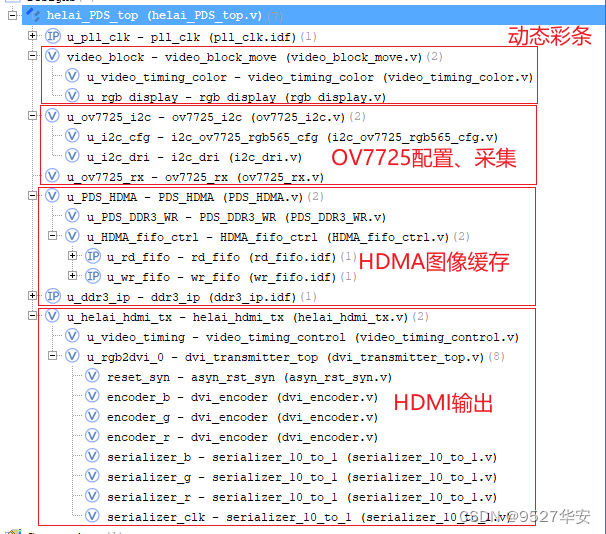
2. Design idea framework
This article uses Unisoc’s PGL22G-6MBG324 FPGA as the basic image and video acquisition system. There are two video sources, which correspond to whether the developer has a camera. One is to use a cheap OV7725 camera; if you don’t have one, If the OV7725 camera or FPGA development board does not have a camera input interface, you can use the dynamic color bar generated inside the code to simulate the camera video; the video source is selected through the `define macro definition at the top level of the code. The OV7725 camera input is used as the video source by default after power-on. ; Provides a set of Pango Design Suite 2021.4 version engineering source code. After the FPGA collects the input video, it uses the HDMA video cache architecture developed by me to send the video to the external DDR3 for caching, and then reads the video and sends it to the HDMI display for display; Engineering design block
diagram as follows:
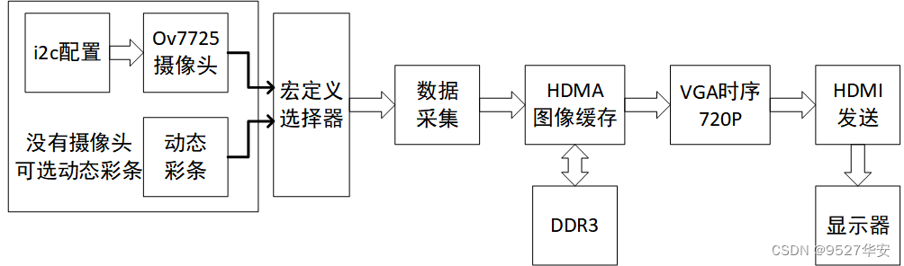
Video source selection
There are two types of video sources, corresponding to whether the developer has a camera in hand. One is to use a cheap OV7725 camera; if you do not have an OV7725 camera or the FPGA development board does not have a camera input interface, you can use the one generated internally by the code. The dynamic color bar simulates camera video; the video source is selected through the macro definition at the top level of the code. The OV7725 camera input is used as the video source by default after power-on; the video source is selected through the `define macro definition at the top level of the code; as follows: Video source
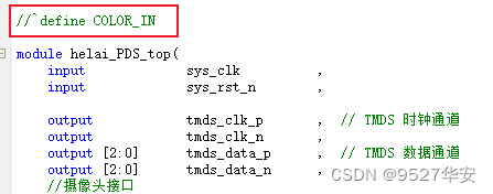
selection The logic code part is as follows:
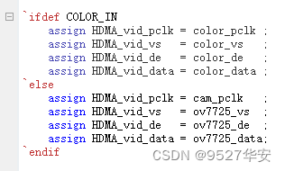
The selection logic is as follows:
when (comment) define COLOR_IN, the input source video is a dynamic color bar;
when (no comment) define COLOR_IN, the input source video is OV7725;
OV7725 camera configuration and collection
The OV7725 camera requires i2c configuration before it can be used. The video data of the DVP interface needs to be collected into RGB565 or RGB888 format video data. Both parts are implemented using the verilog code module. The code location is as follows: The camera is configured with a resolution of 640x480; the camera
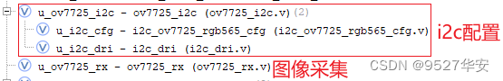
acquisition
module Supports video output in RGB565 and RGB888 formats, which can be configured by parameters, as follows:
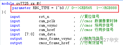
RGB_TYPE=0 outputs the RGB565 format;
RGB_TYPE=1 outputs the RGB888 format;
select the RGB888 format for design;
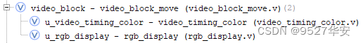
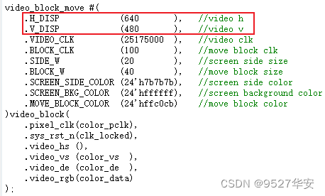
Dynamic color bar
The dynamic color bar can be configured for videos of different resolutions. The border width of the video, the size of the dynamic moving block, the moving speed, etc. can all be parameterized. Here I configure the resolution as 640x480, the code location of the dynamic color bar module and the top-level interface. An example is as follows:
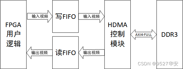
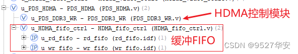
HDMA image cache
The essence of the HDMA image cache is an AXI4-FULL-MASTER bus that encapsulates the user interface. HDMA interacts with DDR3 externally. The user interface of the DDR3 controller that comes with Unisoc Tongchuang FPGA is the AXI4-FULL bus. HDMA instantiates two internally. A FIFO interacts with the internal logic of the FPGA, so when developers use HDMA, they no longer need to worry about the complicated AXI4-FULL protocol, they only need to be as simple as using a FIFO; the HDMA architecture is as follows: the code architecture is as follows
:
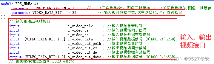
Input and output video
The data format of the input video is RGB, which is the typical VGA video timing in the form of pclk, vs, de, rgb. However, it should be noted that because the input video interacts directly with the FIFO, the data bit width on the AXI side of the FIFO is 128 bits. In order to ensure the correct positioning of data, the RGB signal interface of the input video cannot be the traditional 24-bit. It can be set to 16 or 32-bit. The code is configured through parameters. I configured it to 32-bit, as follows:
HDMA buffer FIFO
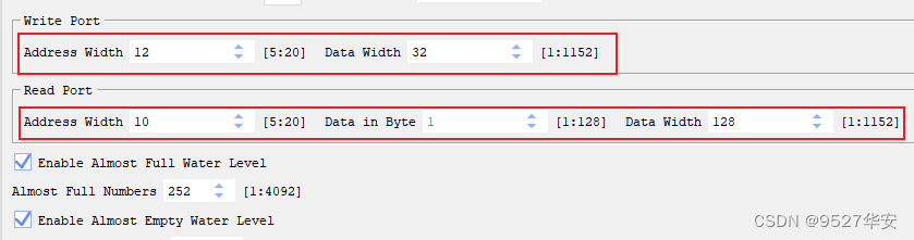
Instantiate two FIFOs as buffers for FPGA logic data and AXI4 data. The so-called buffering refers to the conversion of data bit width, clock domain conversion, control of read and write timing, etc. The data bit width on the FPGA logic side is 32 bits, and AXI4 The data bit width on the side is 128 bits; taking the write FIFO as an example, the configuration is as follows:
HDMA control module
The main function of the HDMA control module is to realize the two major functions of AXI4-FULL host and image cache read and write address switching; AXI4-FULL host is relatively simple, just follow the AXI4-FULL timing diagram and it is done, and image cache read and write address switching is It’s difficult. This design uses top-level parameters to configure the number of frames for the image cache, as follows:
HDMA_PINGPANG_EN=1 means the image will be cached for three frames;
HDMA_PINGPANG_EN=0 means the image will be cached for a single frame;
this design is configured as HDMA_PINGPANG_EN=1;
in order to realize the image Multi-frame cache, segment the read and write addresses as follows:
read and write address = frame address + data address;
data address: the address increment of a normal AXI4 data burst;
write frame address: +1 when a frame of image arrives ;
Read frame address: +2 when a frame of image arrives;
In this way, different frame addresses can be read and written at the same time, and the output image is perfect. . .
This is also called a ping-pong operation. The core code is as follows:

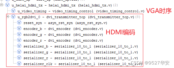
HDMI output
HDMI output includes VGA timing and HDMI encoding modules. VGA timing can only achieve 720P on Ziguang PGL22G-6MBG324 FPGA, because this FPGA may be too low-end to output a 742.5M serial clock. Of course, you use an HDMI encoding chip 1080P can be achieved, so only the output resolution of 720P can be achieved here; the HDMI encoding module is to be implemented using primitives, the same as Xilinx's, and the code structure is as follows:
3. Detailed explanation of PDS project
Development board FPGA model: Unisoc – PGL22G-6MBG324;
Development environment: Pango Design Suite 2021.4
Input: OV7725 camera or dynamic color bar, resolution 640x480;
Output: HDMI, resolution 1280x720;
Engineering role: Unisoc FPGA image video Acquisition system;
the project code structure is as follows:
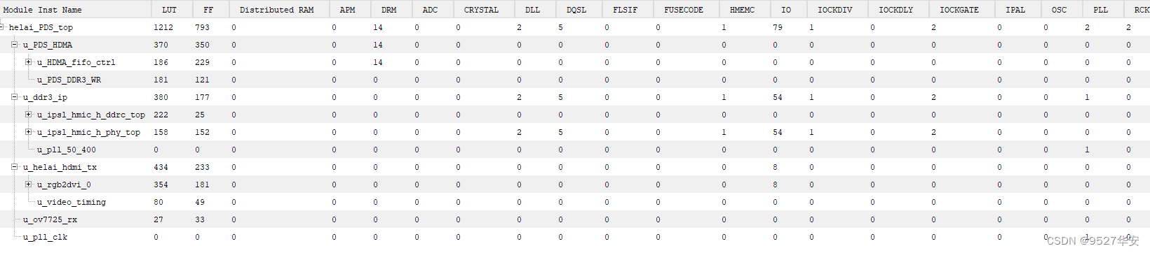
the resource consumption and power consumption of the project are as follows:
4. Board debugging, verification and demonstration
Preparation
You need the following equipment to transplant and test the project code:
1: FPGA development board;
2: OV7725 camera, if not available, choose dynamic color bars;
3: HDMI transmission line;
4: HDMI display, the resolution is required to support 1280x720 ;
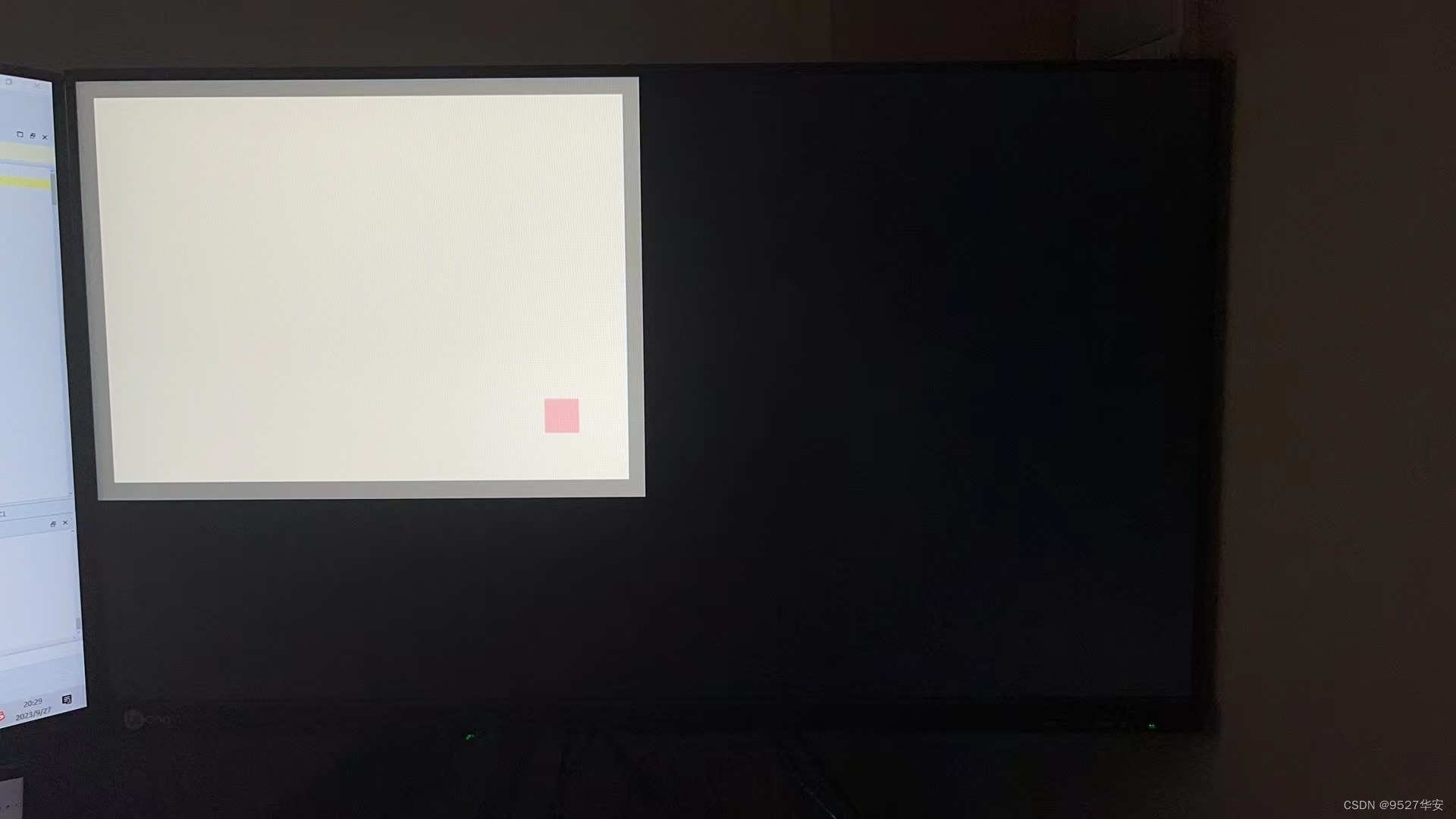
static presentation
The static demonstration of OV7725 input 640x480 resolution HDMI output is as follows: The
static demonstration of dynamic color bar input 640x480 resolution HDMI output is as follows:
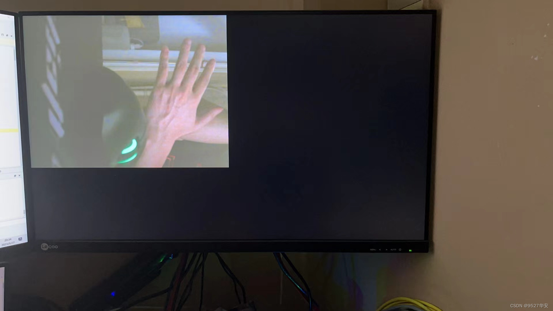
Dynamic presentation
The dynamic video demonstration is as follows:
Unisoc FPGA-OV7725
5. Benefits: Obtain project source code
Bonus: Acquisition of engineering code.
The code is too large to be sent by email. It will be sent via a certain network disk link.
The information acquisition method is: private, or the V business card at the end of the article.