Table of contents
1 Introduction
There are currently two schemes for FPGA to implement SDI video codec:
one is to use a dedicated codec chip, such as a typical receiver GS2971, and a transmitter GS2972. The advantage is simple. For example, GS2971 directly decodes SDI into parallel YCRCB. The disadvantage is that it costs more High, you can check the price of GS2971 on Baidu;
another solution is to use FPGA to implement encoding and decoding, and use FPGA's GTP/GTX resources to implement deserialization. The advantage is that FPGA resources are used reasonably, and GTP/GTX resources are unnecessary. It is more difficult and requires a higher level of FPGA; my homepage has an SDI column, which contains some project source codes using FPGA's GTP/GTX resources;
This article describes in detail the implementation design scheme for FPGA to send and receive SDI video based on GS2971/GS2972. After the project code is compiled and passed, it will be debugged and verified on the board. There is a demonstration video at the end of the article, which can be directly transplanted. , is also suitable for on-the-job engineers to do project development, and can be applied to the fields of digital imaging and image transmission in medical, military and other industries; provide
complete and smooth engineering source code and technical support;
the acquisition method of engineering source code and technical support is placed in At the end of the article, please be patient to see the end;
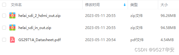
This design provides two sets of vivado projects;
one is GS2971 decoding SDI video, which is output by HDMI after DDR image buffering; SDI 1080P@30Hz frame video input; 1080P@60Hz frame output; the second
is GS2971 decoding SDI video, after DDR image buffering SDI output encoded by GS2972; SDI 1080P@30Hz frame video input; SDI 1080P@30Hz frame output;
2. My existing SDI codec scheme
There is an SDI video column on my blog homepage, which is full of FPGA codec SDI project source code and blog introduction; there are both SDI codecs based on GS2971/GS2972 and SDI codecs based on GTP/GTX resources; column address link: https://blog.csdn.net/qq_41667729/category_12243350.html?spm=1001.2014.3001.5482
3. Interpretation of GS2971/GS2972 chip
Interpretation of GS2971
GS2971 is an SDI decoding chip, which decodes the input SDI video to yuv422 video output; the block diagram of the GS2971 data sheet is as follows: The GS2971 data
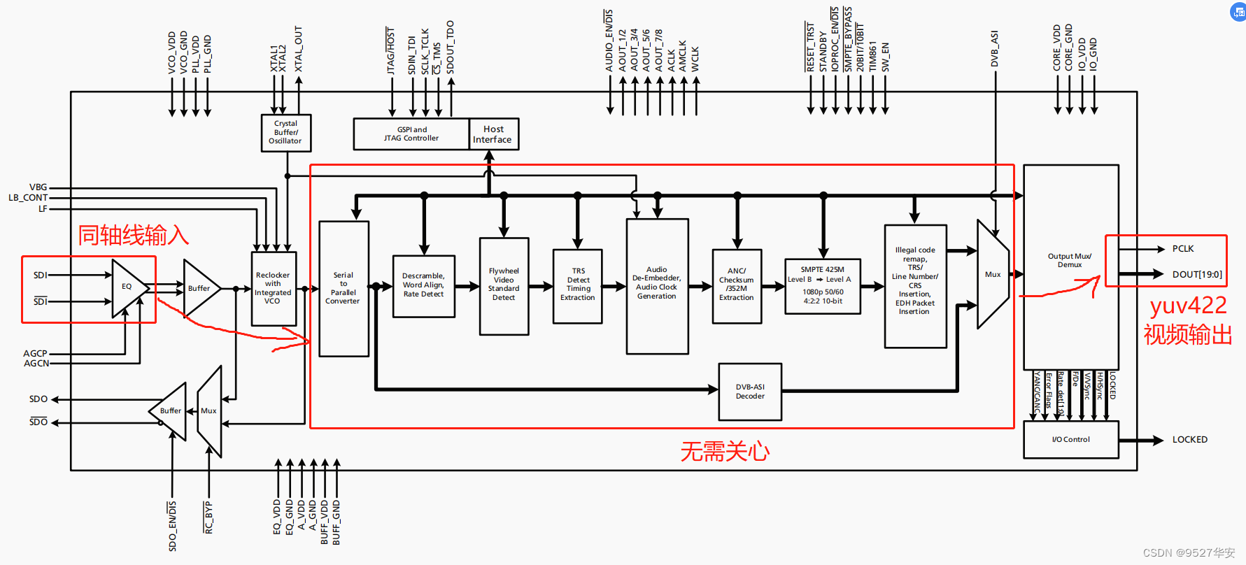
sheet has 152 pages, but as an FPGA developer, most of them are nonsense, we only need to care The input and output formats of the video are sufficient;
as can be seen from the above figure, the input of GS2971 is SDI video, and the output is yuv422 video stream; we don’t need to care about the decoding and conversion process in the middle, this is the charm of digital IC, which encapsulates complex circuits into dedicated IC, users only need to read the manual to use it like a fool;
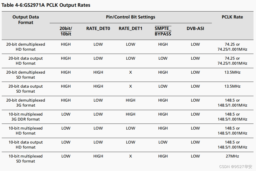
the output yuv422 video stream belongs to VGA video format, with pixel clock PCLK, horizontal synchronization signal HS, vertical synchronization signal VS, valid data signal DE, 20-bit pixel data DOUT; GS2971 The output video is directly related to the input SDI video rate. Taking 3G-SDI as an example, when 3G-SDI is input, the output video pixel clock is 148.5M. For details, see the screenshot in the manual: In addition, GS2971 does not need software configuration, and the resistor can be pulled up and down
. Complete the configuration, this part is what the hardware engineer who draws the schematic diagram cares about, so I won’t say more;
Interpretation of GS2972
The role of GS2972 is exactly the opposite of GS2971. It is an SDI encoding chip that encodes the input yuv422 video to SDI video output; the chip also does not require software configuration, so I won’t say more here;
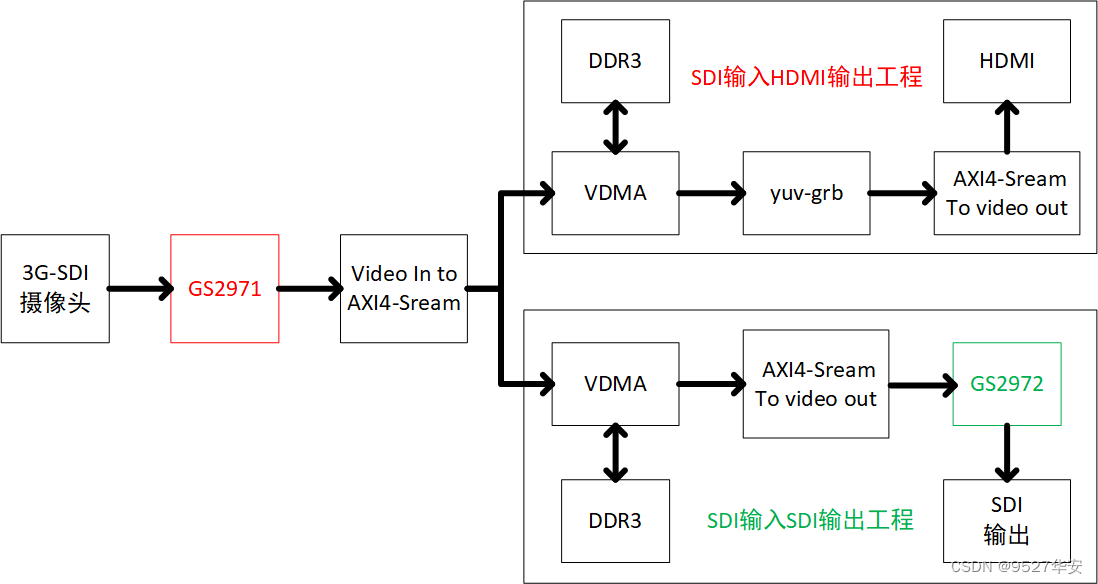
4. Detailed design plan
This design provides two sets of projects;
project 1: SDI input, buffer DDR3 after decoding by GS2971, and finally output via HDMI;
project 2: SDI input, buffer DDR3 after decoding by GS2971, and finally output SDI after encoding by GS2971; the
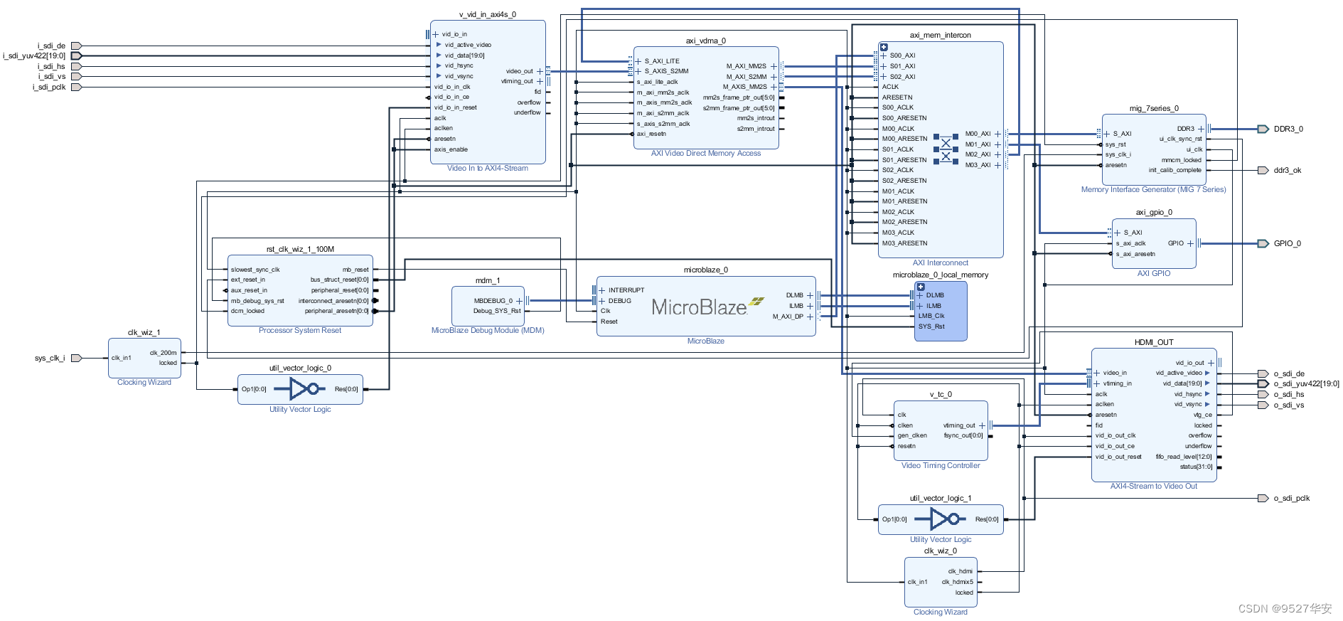
design block diagram is as follows : The two projects are drawn together in the block diagram;
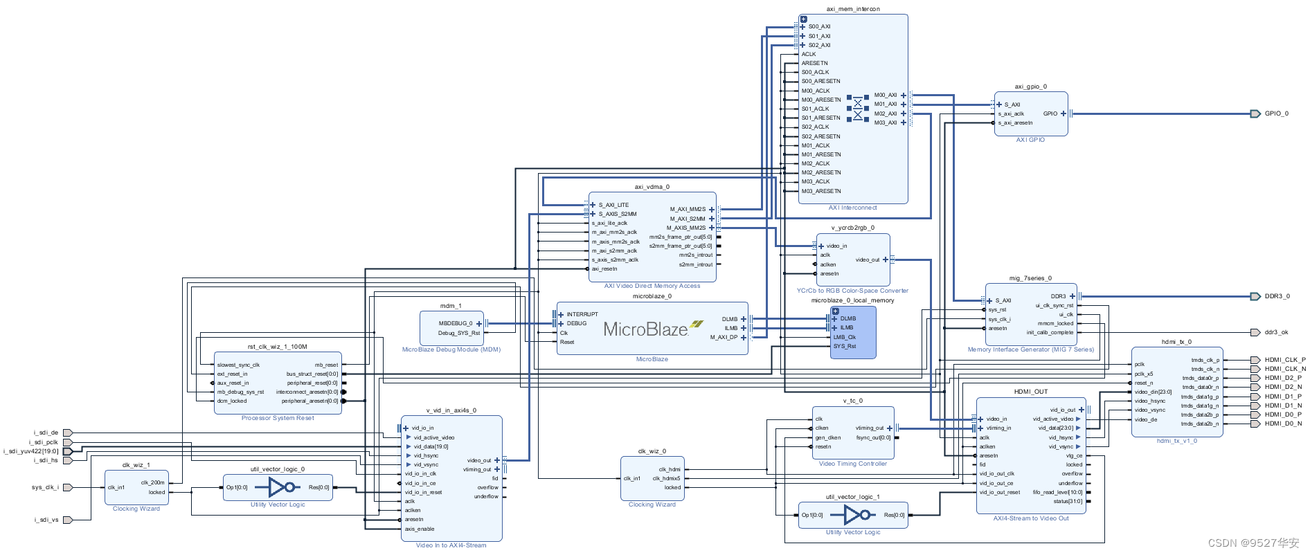
5. Interpretation of vivado project 1
Hardware Logic Engineering
Development board FPGA model: Xilinx–xc7k325tffg676-2;
development environment: Vivado2019.1;
input: 3G-SDI video;
output: HDMI, 1080P;
The engineering block design is as follows:
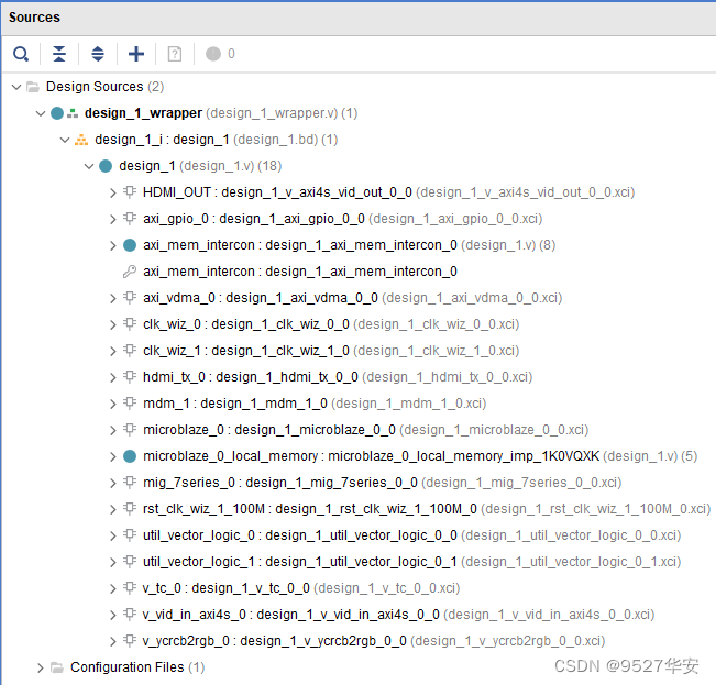
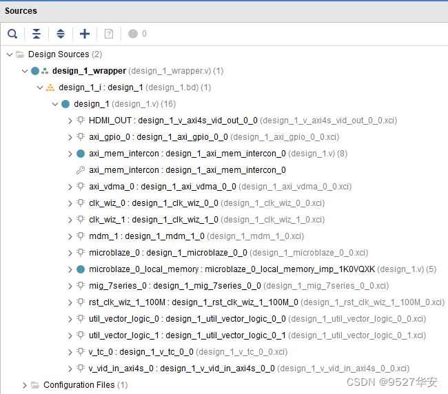
the engineering code structure is as follows:
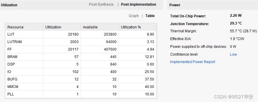
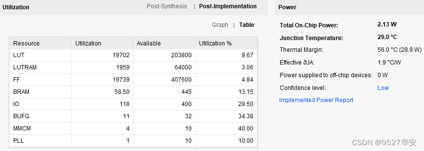
the resource consumption and power consumption estimation are as follows:
Software SDK Engineering
The software SDK project is as follows: only VDMA configuration is done;
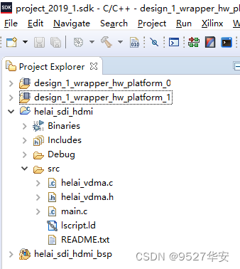
the main function is as follows:
#include <stdio.h>
#include "xgpio.h"
#include "unistd.h"
#include "helai_vdma.h"

XGpio_Config *XGpioCfg;
XGpio led_gpio;
#define	AXI_GPIO_DEVICE_ID	XPAR_GPIO_0_DEVICE_ID

int main(){


	XGpioCfg = XGpio_LookupConfig(AXI_GPIO_DEVICE_ID);
	XGpio_CfgInitialize(&led_gpio, XGpioCfg, XGpioCfg->BaseAddress);
	XGpio_SetDataDirection(&led_gpio, 1, 0);	//output
	XGpio_DiscreteWrite(&led_gpio, 1, 0);
	helai_vdma();
	while(1){


		usleep(500000);
		XGpio_DiscreteWrite(&led_gpio, 1, 1);
		usleep(500000);
		XGpio_DiscreteWrite(&led_gpio, 1, 0);
	}
}
6. Interpretation of vivado project 2
Hardware Logic Engineering
Development board FPGA model: Xilinx–xc7k325tffg676-2;
development environment: Vivado2019.1;
input: 3G-SDI video;
output: 3G-SDI video;
The engineering block design is as follows:
the engineering code structure is as follows:
the resource consumption and power consumption estimation are as follows:
Software SDK Engineering
The software SDK project is as follows: only VDMA configuration is done;
the main function is as follows:
#include <stdio.h>
#include "xgpio.h"
#include "unistd.h"
#include "helai_vdma.h"

XGpio_Config *XGpioCfg;
XGpio led_gpio;
#define	AXI_GPIO_DEVICE_ID	XPAR_GPIO_0_DEVICE_ID

int main(){


	XGpioCfg = XGpio_LookupConfig(AXI_GPIO_DEVICE_ID);
	XGpio_CfgInitialize(&led_gpio, XGpioCfg, XGpioCfg->BaseAddress);
	XGpio_SetDataDirection(&led_gpio, 1, 0);	//output
	XGpio_DiscreteWrite(&led_gpio, 1, 0);
	helai_vdma();
	while(1){


		usleep(500000);
		XGpio_DiscreteWrite(&led_gpio, 1, 1);
		usleep(500000);
		XGpio_DiscreteWrite(&led_gpio, 1, 0);
	}
}
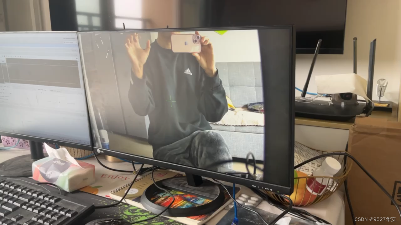
7. Board debugging and verification
Take project 1 as an example, SDI input, HDMI output effect is as follows:
8. Benefits: Acquisition of engineering codes
Benefits: Obtaining the engineering code
The code is too large to be sent by email, and it is sent by a link to a certain network disk.
Data acquisition method 1: private, or the V business card at the end of the article.
Data acquisition method 2: XX number at the end of the article, reply 001009
network disk data is as follows: