Table of contents
- 1 Introduction
- 2. My existing SDI codec scheme
- 3. My existing PCIE solution
- 4. PCIE based on zynq architecture
- 5. Overall design idea and scheme
- 6. Detailed explanation of vivado project
- 7. Driver installation
- 8. QT host computer software
- 9. Board debugging and verification
- 10. Welfare: acquisition of engineering code
1 Introduction
PCIE (PCI Express) adopts the current popular point-to-point serial connection in the industry. Compared with the shared parallel architecture of PCI and earlier computer buses, each device has its own dedicated connection. It does not need to request bandwidth from the entire bus, and it can Improving the data transmission rate to a very high frequency and achieving the high bandwidth that PCI cannot provide is the preferred direction of high-speed interfaces in various industries at present, and has high practical value and learning value;
This design uses Xilinx's official XDMA solution to build a PCIE communication platform based on Xilinx series FPGAs. This solution is only applicable to Xilinx series FPGAs. It also provides XDMA installation drivers and QT host computer source codes, eliminating the need to use XDMA tedious drivers. I am at a loss for finding and developing PC software, and building a vivado project, saves the embarrassment of not knowing how to use XDMA, making the use of PCIE easy to use, without having to care about its complicated PCIE protocol; because I The development board only supports PCIE X8, so the code provided is PCIE X8 architecture. If you need friends with PCIE X1, X2, X8, X16, X32, you can modify this project by yourself, or follow me, I will release new projects in real time .
This project realizes the basic PCIE communication, and conducts a speed test with the QT host computer.

This article describes in detail the implementation design scheme of Zynq pure verilog decoding SDI video and sending PCIE to the host computer to use QT to capture video in real time. Using the SDI input interface that comes with the development board, real-time capture HDMI input video, after buffering DDR3, all the way through HDMI output The chip outputs the display, and the other channel passes through XDMA, and sends it to the QT host computer display program through PCIE; to achieve the synchronous operation of SDI capture video loop output and PCIE output to computer display, which belongs to the high-end project in the field of FPGA image acquisition. . .
After the project code is compiled and passed, it is debugged and verified on the board. There is a demonstration video at the end of the article, which can be directly transplanted into the project. It is suitable for students in school to do graduation design, graduate project development, and also for in-service engineers to do project development. It can be applied to medical, military, etc. The field of digital imaging and image transmission in the industry;
provide complete and smooth engineering source code and technical support;
the method of obtaining engineering source code and technical support is at the end of the article, please be patient to the end;
2. My existing SDI codec scheme
There is an SDI video column on my homepage, which includes SDI codecs based on FPGA pure logic resources, including GTX-based codecs and GTH-based codecs, and SDI video transceiver projects based on GS2971/GS2972, as well as ordinary SDI Accept and send, there are also SDI video scaling, splicing, UDP transmission, SFP optical fiber transmission, PCIE transmission, etc.; the following is the column address:
click to go directly
3. My existing PCIE solution
My homepage has a PCIE communication column, which includes PCIE solutions based on RIFFA and PCIE solutions based on XDMA; simple data interaction, speed measurement, and application-level image acquisition and transmission; both pure FPGA PCIE and PCIE of zynq; the following is the column address:
click to go directly
4. PCIE based on zynq architecture
For the theoretical part of PCIE, you can learn theoretical knowledge from Baidu or csdn or Zhihu. In fact, XDMA is used, and there is no need for complex protocols and theories until PCIE. . .
Here we will focus on the PCIE design method based on the zynq architecture;
we know that for data interaction between PCIE and the PC, the DDR memory attached to the FPGA must be used as an "intermediary"; but the FPGA of the zynq architecture has a characteristic, its PL and DDR can be installed on the PS side, so can the DDR on both sides be used as the "intermediary" of PCIE communication? Obviously, it is impossible to have both fish and bear's paws;
let's take a look at the HP bus of zynq first. The highest bit width of HP is only 64 bits, as follows:
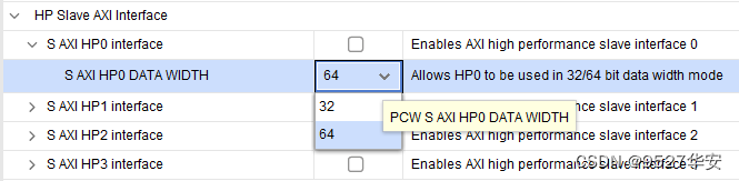
If the reference clock given by zynq to PL is 150M, then the total bandwidth of HP is 150000000x64=9.6 Gb; even if the reference clock is increased to an astonishing 200M, then the total bandwidth of HP is 200000000x64=12.8Gb; while the PCIE2.0 single Line speed of XDMA is 5Gb, and the total speed of PCIEX8 is 5x8=40Gb; It is impossible for PS side DDR as the "intermediary" of PCIE and PC communication to meet the loan requirements. In addition, due to coding, protocol and other expenses, the available bandwidth can only reach 80%, and PS side DDR is even more impossible, so we can only choose PL The side DDR is used as the "intermediary" of PCIE and PC communication;
let's see why the PL side DDR can:
PL side calls MIG, the user operation clock of MIG is 200M, and the AXI data bit width is 256 bits, so the theoretical bandwidth=200000000x256=51.2 Gb; actual bandwidth = 51.2x80% = 40.96Gb; just enough to meet the 40Gb line rate of PCIEX8 2.0;
such a detailed calculation tells you the reason for choosing the PL side DDR of zynq, which is enough for nanny-level teaching. . .
5. Overall design idea and scheme
The overall design idea and scheme are as follows:

SDI camera
The output video resolution of the SDI camera I used is 1080P@30Hz; it varies according to different cameras;
Gv8601a single-ended slip
Gv8601a has the function of equalizing EQ. The reason for choosing Gv8601a here is that it copied the official Xilinx board. Of course, other types of devices can also be used.
GTX deserialization
GTX is responsible for deserialization, decomposing the original SDI video into 20-bit parallel data. My board is K7, so I use GTX. If it is an A7 board, I use GTP. Here, GTX does not call IP, but directly calls GTXE2_CHANNEL and GTXE2_COMMON source language, which can be said to use Xilinx’s GTX resources to the extreme level, is worth reading carefully. In fact, calling IP is nothing more than making the call source language interface-like. Directly calling the source language may have a deeper understanding. This point, You can't learn it in the so-called FPGA tutorials on the market.
SDI decoding
Calling the SMPTE-SDI IP core implementation, GTX only decodes the high-speed serial data into parallel, but does not parse the SDI protocol, and the SMPTE-SDI IP core completes the decoding of the SDI protocol, removing the packet information and control in the SDI protocol information, parse out valid video data, and for detailed SMPTE-SDI IP core interface definitions, please refer to the official manual;
VGA timing recovery
The function of this module is to decode and restore the hs, vs and de signals, that is, restore the normal VGA video timing;
to restore the normal VGA video timing, you must first understand the following picture:
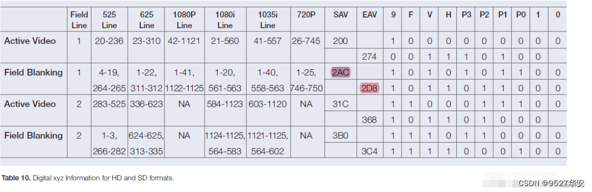
According to this table, the image timing can be restored , look at the code specifically, one or two sentences here are really unclear, if you want to fully explain it, it is more than enough to write 5 books;
YUV to RGB
It's simple here, YUV4:4:4 to RGB8:8:8, a few formulas and a few lines of code are low-end operations; so far, the
SDI decoding process is completed, and the next step is the image output process;
For the specific explanation of the principle of SDI decoding, please refer to my previous article: Click to go directly
image cache
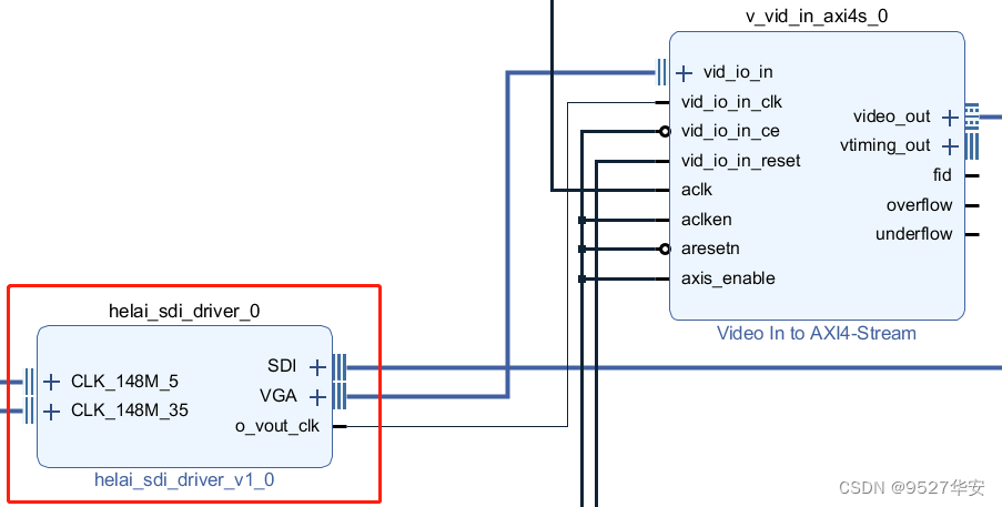
This design uses VDMA as a cache, and VDMA is configured through zynq's SDK;
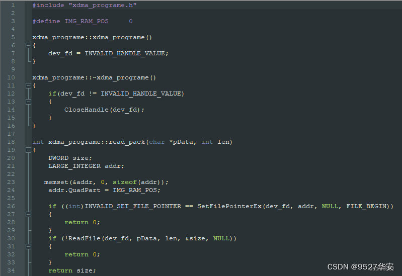
PCIE send channel
Calling Xilinx official XDMA as the PCIE transmission engine does not need to understand the complex protocol of PCIE. XDMA integrates the AXI4 interface and directly interacts with DDR3. The user can read and write data through the specified address of DDR3; the specific principle of the PCIE transmission channel is explained
. Please refer to my previous article: Click to go directly
SDI sync output path
After the SDI video is captured and cached, read out the data and send it to the HDMI output. This step can be used as a reference for the QT host computer. The synchronous output can compare the correctness of PCIE video transmission. Some projects also have the need for synchronous output of PCIE and HDMI, so here is the design It must be very close to the real project. . .
HDMI transmission uses ADV7511 chip, ADV7511 needs i2c configuration to use; this design uses zynq configuration;
6. Detailed explanation of vivado project
Development board FPGA model: Xilinx–zynq–xc7z100ffg900-2;
development environment: Vivado2019.1;
input: 3G-SDI; resolution 1920X1080@30Hz;
output 1: PCIE X8 to the computer QT host computer;
output 2: HDMI output; Resolution 1920X1080@60Hz;;
Application: SDI video capture card;
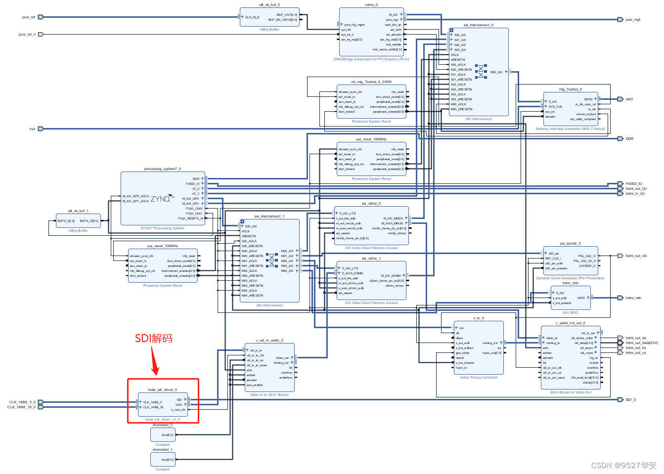
Project BD is as follows: The
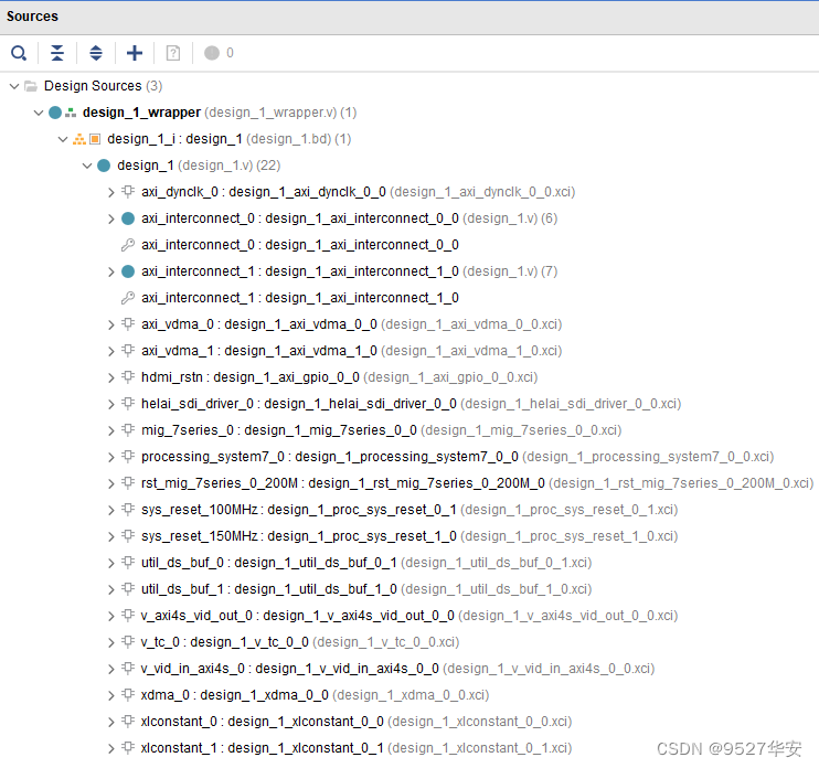
integrated project code structure is as follows:
The source code of the SDI decoding part is as follows:
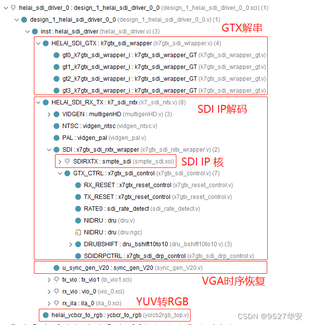
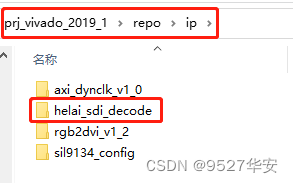
The location of the source code of the SDI decoding part is shown in the figure:
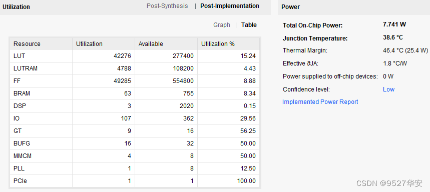
FPGA resource consumption and power consumption The estimated consumption is as follows:
7. Driver installation
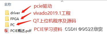
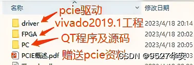
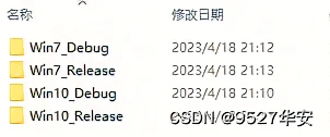
Provide Win system driver, the directory is as follows:
Driver installation refers to the previous speed test: click to go directly
8. QT host computer software
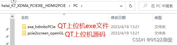
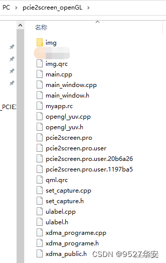
QT display host computer: provide source code and executable program, the released version is QT5.6.2; the location is as follows:
9. Board debugging and verification
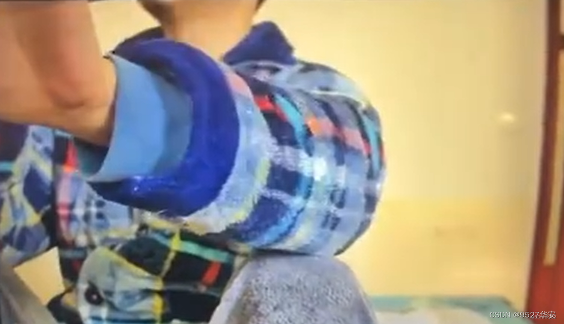
SDI Sync HDMI Output Verification
PCIE output verification
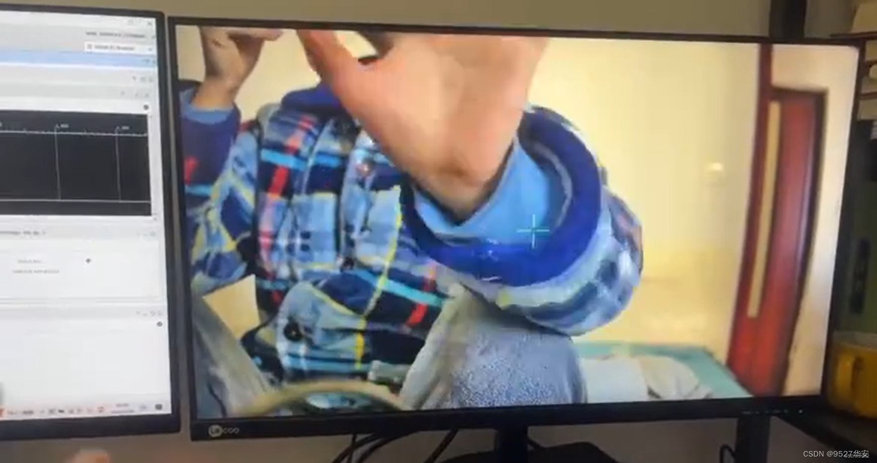
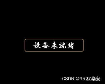
Open the host computer test program for PCIe display test, open the display software pcie2screen as shown in the figure below, the software is in the following location, the experimental results are as follows: After turning on the

host computer, you can see that the software pauses playback:
click the middle button to start playing the SDI input video source video:
10. Welfare: acquisition of engineering code
Benefits: Obtaining the engineering code
The code is too large to be sent by email, and it is sent by a link to a certain network disk.
Data acquisition method 1: private, or the V business card at the end of the article.
Data acquisition method 2: XX number at the end of the article, reply 001007
network disk data is as follows: