Table of contents
1 Introduction
At present, the basic ecology of udp implemented by fpga on the Internet is as follows:
1: udp transceiver written in verilog, but without ping function, such code function can be used normally, but without ping function, it is basically waste, and will not be used in actual projects Such a code, just imagine, multi-machine interconnection, if there is a problem, your network card does not have a ping function, and you don’t even have a basic troubleshooting mechanism. Who would dare to use such a code?
2: The udp transceiver with ping function, the code is excellent and easy to use, but it is basically not open source, and the source code will not be provided to you. This kind of code also has shortcomings, that is, if there is a problem, I don’t know how to troubleshoot it. ;
3: Using Xilinx's Tri Mode Ethernet MAC triple-speed network IP implementation, this code is also very good, but still the same problem, there is no source code, and the triple-speed network IP needs a license, the triple-speed network IP has realized rgmii to gmii and then Conversion to axis;
4: Use FPGA’s GTX resource to use SFP optical port to realize UDP and communication. This kind of solution can be completed without external network transformer. This solution is such a design;
This design uses Milink's UDP protocol stack to realize the MAC layer design of UDP communication, and calls Xilinx's official 10G Ethernet Subsystem IP core to realize the function of a network transformer, so as to realize the UDP communication solution without an external network chip, which is easy to implement The current popular 10G 10G network communication; the UDP protocol stack of Millink is not open source at present, and only provides netlist files, but it does not affect the use. The protocol stack has a user interface, so that users do not need to care about the complicated UDP protocol. You only need to care about the simple user interface timing to operate UDP sending and receiving, which is very simple; this design realizes the loopback sending and receiving of UDP data through a fifo, and uses the network debugging assistant on the computer side to verify UDP sending and receiving;
This design links 2 SFP optical ports, one is configured as a UDP server, and the other is configured as a client; this design is stable and reliable after a large number of repeated tests, and can be directly transplanted and used in projects. The project code can be comprehensively compiled and debugged on the board, which can be directly Project transplantation, suitable for project development of students and graduate students, and also suitable for project development of in-service engineers, can be applied to the digital communication field of medical, military and other industries; provide complete and smooth engineering source code and technical support; engineering
source
code The method of obtaining and technical support is placed at the end of the article, please be patient to read the end;
2. The UDP scheme I have here
At present, I have the following UDP solutions and application examples:
My blog home page has a FPGA Ethernet communication column, which is free, and there are many UDP applications implemented by FPGA, including conventional gigabit network and 10 gigabit network solutions , brothers who have needs for network communication can go and have a look: click directly to go
3. Detailed design plan
Before talking about the design scheme, let’s take a look at what conditions the FPGA should have to implement the UDP communication scheme, which is roughly as follows:
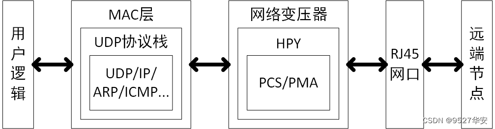
1: User logic:
The actual data that the developer needs to send and receive can exist in various forms, such as custom format, AXIS The data flow format and so on, the interface timing of the user logic must be consistent with the interface timing of the MAC layer;
2: The MAC layer
is mainly composed of specific protocol logic such as UDP, IP, ARP, ICMP, etc., to realize the grouping and unpacking of network data, It is equivalent to doing what Sockte does in the software. Sockte relies on the CPU to make network data packets, and the MAC layer here directly uses hardware resources to make network data packets, which liberates the enslavement of network data packets to the CPU. In today's fashionable RDMA perfectly reflected in. . . The MAC layer of this design uses Milink’s UDP protocol stack. For this part, please refer to my previous article
3: The network transformer
is mainly composed of PCS/PMA. PCS mainly realizes the encoding and decoding of parallel data, such as the classic 8b/ 10 encoding and decoding, PMA mainly realizes parallel/serial/serial parallel conversion, the output interface is a high-speed differential signal, which can be directly connected to SFP or RG45 network port; 4: RJ45 network port:
commonly known as crystal head, plugged into the network cable. . .
5: Remote node
The FPGA development board can be understood as a network card, and the remote node is another network card connected to it;
The difference between this design and the above-mentioned traditional FPGA implementation UDP solution is the network transformer part. The previous network transformer is a real network PHY chip, such as the RTL8211, B50610, 88E1518, etc. I often use; this design does not use the network transformer, but It is to call Xilinx official 10G Ethernet Subsystem IP core to realize the function of network transformer, and realize the connection with the remote node through SFP optical port output. The design block diagram is as follows: This design uses the network debugging assistant on the computer side to communicate with the development board to realize
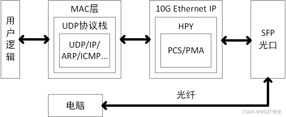
UDP For the data loopback test, this design does not use an external network transformer, but calls Xilinx's official 10G Ethernet Subsystem IP core, which is completed in the form of SFP optical port output.
Here we will focus on Xilinx's official 10G Ethernet Subsystem IP core;
pay attention! ! !
The 10G Ethernet Subsystem IP core is only available in K7 and above FPGAs.
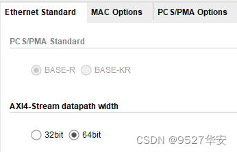
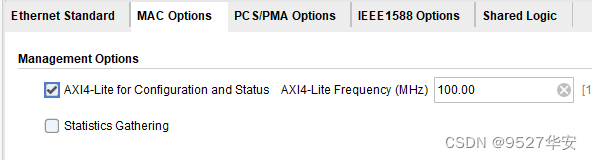
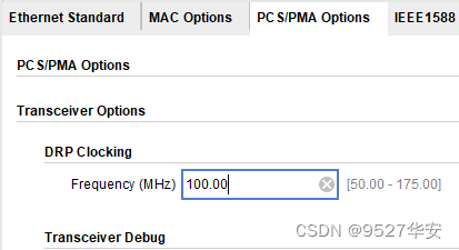
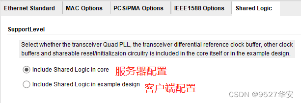
The IP configuration is as follows:
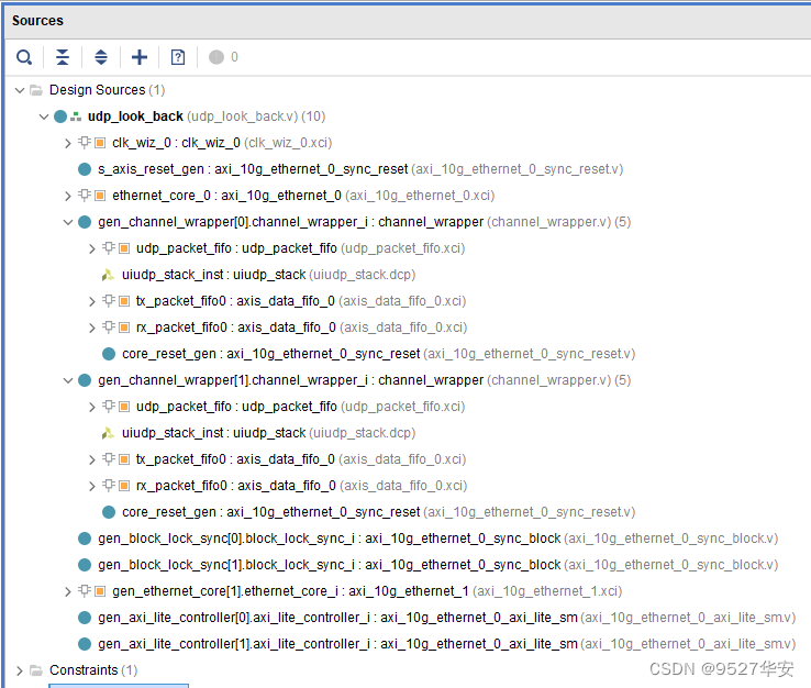
4. Detailed explanation of vivado project
Development board FPGA model: Xilinx xc7k325tffg900-2;
development environment: vivado2020.2;
input/output: SFP optical port;
network card speed: 10G;
test items: UDP data loopback, ping, etc.;
FPGA resource consumption and power consumption after comprehensive compilation Estimates are as follows:

5. Board debugging verification and demonstration
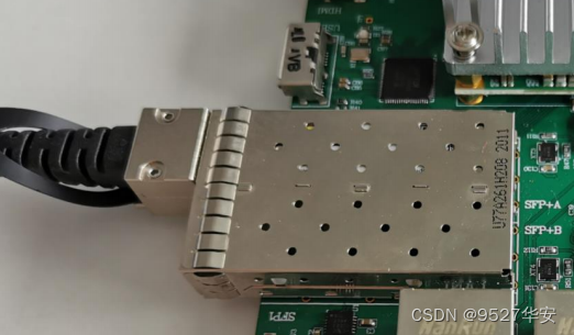
You need to buy a SFP-to-RJ45 module to insert into the SFP optical port, and then use a network cable to connect the development board and the computer, as follows:
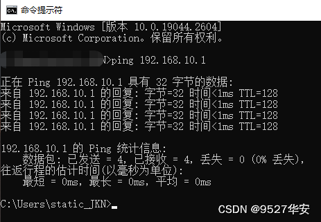
After the board is powered on and the bit is downloaded, first test the ping function, as follows:
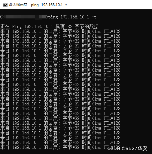
a single ping is not enough, directly perform continuous ping, as follows :
Then use the network debugging assistant to perform the data sending and receiving test, as follows:
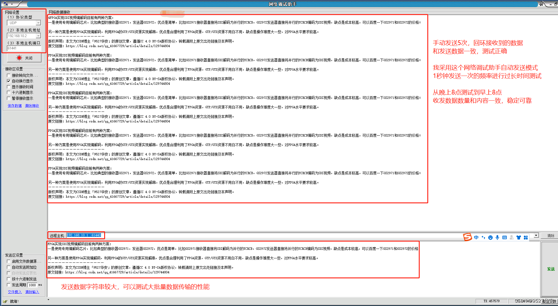
there are both manual sending and receiving tests, and there is also a long-term sending and receiving test with a cycle of 12 hours, and there is no packet loss in the test results. . .
The speed measurement is as follows:

Observe the sending rate of the Ethernet port of the development board on the computer. This speed measurement only represents the highest possible speed, and does not represent the real speed of the computer without packet loss. The point-to-point non-packet loss speed of UDP and the network card of the computer , CPU speed, memory speed, operating system all matter. . .
6. Welfare: acquisition of engineering code
Benefits: Obtaining the engineering code
The code is too large to be sent by email, and it is sent by a certain degree network disk link. The
method of data acquisition: private, or the V business card at the end of the article.
The network disk information is as follows: