9.Declaring wires | wire decl
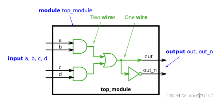
problem:Implement the following circuit. Create two intermediate wires (named anything you want) to connect the AND and OR gates together. Note that the wire that feeds the NOT gate is really wire out, so you do not necessarily need to declare a third wire here. Notice how wires are driven by exactly one source (output of a gate), but can feed multiple inputs.
If you’re following the circuit structure in the diagram, you should end up with four assign statements, as there are four signals that need a value assigned.
`default_nettype none
module top_module(
    input a,
    input b,
    input c,
    input d,
    output out,
    output out_n   );

    wire ab_out;
    wire cd_out;
    wire abcd_out;
    assign out = (a & b) | (c & d);
    assign out_n = ~((a & b) | (c & d));

endmodule
注:
1、`default_nettype none 在后面Vectors中会提到
2、当运行完之后 ,突然发现定义的ab_out、cd_out、abcd_out三根线并没有用上(当时真是没用心,就是简单的循规蹈矩的去做,没做思考),我把三条语句删去之后,运行也是通过的。当然从逻辑上即使不运行这当然是通的。但这样虽然省了代码行数,但如果后面还有继续的电路图,那么这样每行代码的逻辑就会很复杂,也不符合模块化的思想。
因为期望代码行数为5,那么经过改进,如下。
`default_nettype none
module top_module(
    input a,
    input b,
    input c,
    input d,
    output out,
    output out_n   );

    wire ab_out, cd_out;   //可以直接连续赋值
    assign ab_out = a & b;
    assign cd_out = c & d;
    assign out = ab_out | cd_out;
    assign out_n = ~out;

endmodule
答案很不唯一,可自行多尝试
10. 7458 chip
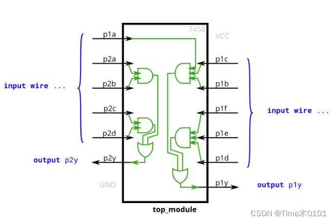
problem:Create a module with the same functionality as the 7458 chip. It has 10 inputs and 2 outputs. You may choose to use an assign statement to drive each of the output wires, or you may choose to declare (four) wires for use as intermediate signals, where each internal wire is driven by the output of one of the AND gates. For extra practice, try it both ways.
问题部分说了两种方式,我们都来试一下。
然后要求的是2到10行
1、You may choose to use an assign statement to drive each of the output wires,
那就试一下,只用2行,就像上一题一样,一行直接把逻辑表达完整。
assign p1y = (p1a & p1b & p1c) | (p1f & p1e & p1d);
assign p2y = (p2a & p2b) | (p2c & p2d);
2、or you may choose to declare (four) wires for use as intermediate signals, where each internal wire is driven by the output of one of the AND gates.
	wire and1, and2, and3, and4;

    assign and1 = p1a & p1b & p1c;
    assign and2 = p1f & p1e & p1d;
    assign and3 = p2a & p2b;
    assign and4 = p2c & p2d;

    assign p1y = and1 | and2;
	assign p2y = and3 | and3;