The main reference https://www.eefocus.com/liu1teng/blog/12-02/237897_4533d.html , Xilinx UG471, UG472 and some questions and answers on Xilinx Forum, expressed gratitude in this together.
------------------------------------------------------------------------------------------------------
This paper is mainly used to record free to look a little content on FPGA dedicated clock pins related to recent constraints in doing FPGA project at hand when it came to the document, intended to sort out ideas, save the learning outcomes, as well as others for your own future reference.
The cause was doing when timing constraints file exceptions to the constraints of the content part, we found an FPGA timing exception constraints of many units in the project before the constraint files that often occur are:
set_property CLOCK_DEDICATED_ROUTE FALSE [get_nets NETS_NAME_IBUF]
Object constraints often sys_clk addition, the number of the external communication interface, such as incorporated IBUF line SPI clock pin or MDIO interface.
If you do not add this constraint, when executed implement often it will report error or critical warning, the content will be mentioned together with this constraint, it would be a serious warning or error downgraded to general warning, but has not understood that in the end how it is, so these two days through the document and forums, be made clear ballpark.
That there are a class of pins dedicated clock pins on the FPGA, for they generally introduced FPGA external clock signal, a clock signal and using these Module1 introduced in the FPGA. However, if the design of pin assignments, not doing enough, or pin, then it is possible that access to this dedicated clock signal pin (or called global clock pins), and received the ordinary IO port, so only Add CLOCK_DEDICETED_ROUTE FLASE can bypass the checks PAR, but does not solve the fundamental problem.
In daily contact with many of the Xilinx 7 series FPGA chip, the staff on the Xilinx forum for this is explained this way:
If you are bringing the the clock onto the device then you need to use the CCIO (Clock capable inputs) . Every 7 series FPGA has four clock-capable inputs in each bank. Two of the four are Multi-Region Clock Capable (MRCC) and the other two are Single Region Clock Capable (SRCC). These inputs are regular I/O pins with dedicated connections to internal clock resources.
That is, the chip must be used MRCC or SRCC pin to the external clock signal into the FPGA, and then introduced in the use of these clocks on the FPGA.
For the meaning and connection of both the front and rear stages, described in detail in the table1-1 in UG472:

About the difference between the two, in xilinx forum of https://forums.xilinx.com/t5/Embedded-Processor-System-Design/MRCC-or-SRCC/mp/787546
The following have been answered in detail:
The clock capable pins in a 7 series FPGA serve two purposes; access to the local clocking resources and access to the global clocking resources.
If you are using the global clocking resources (BUFG, BUFH, MMCM, PLL) then the MRCC and SRCC have exactly the same capability - there is no difference between the two.
If you are using the local clocking resources (BUFR and BUFIO), then then the SRCC and MRCC can both only drive only the BUFIO and BUFR located in the same clock region. The BUFIO can then only drive the IOB flip-flops and high speed clock of the ISERDES in the same I/O bank and the BUFR can clock all the logic (except the high speed clock of the ISERDES) in the same clock region.
The only difference between the SRCC and MRCC is that the MRCC can also drive the BUFMR. The BUFMR can then drive the BUFIO/BUFR in the same clock region as well as in the clock regions above and below the MRCC. This would generally be used for "ChipSync" (source synchronous) interfaces that need to use more pins than are available in one I/O bank.
Also in https://forums.xilinx.com/t5/Other-FPGA-Architectures/LVDS-CLK-PN-be-routed-to-MRCC-SRCC-or-regular-differential-IOs/mp/913220 answer under also mentioned:
MRCCs can access multiple clock regions and the global clock tree. MRCCs function the same as SRCCs and can additionally drive multi-clock region buffers (BUFMR) to access up to three clock regions.
Other authors also mentioned:
if you are forwarding clock out from the device, then you can use any regular IOs, I.e
Clock path is
Clock you want to forward -> ODDR -> OBUFDS ->Routed to any regular differential pair .
Here it is to say, if you need an external clock introduced FPGA, but not to use the signal inside the module FPGA as a clock, but only to the introduction of the clock to make a relay or forward, you do not need to take him the MRCC / SRCC pin (though these two types of pins, in general, not to pin the clock when introduced, can also be used as a general IO), but only with an ordinary receiving any IO can be.
There is also noted that if you do clock relay, scheme used is selected ODDR-OBUFDS, both of which are described in UG471 document.
UG471-P128:
Clock Forwarding
Output DDR can forward a copy of the clock to the output. This is useful for propagating
a clock and DDR data with identical delays, and for multiple clock generation, where every
clock load has a unique clock driver. This is accomplished by tying the D1 input of the
ODDR primitive High, and the D2 input Low. Xilinx recommends using this scheme to
forward clocks from the FPGA logic to the output pins.
Further, in the table2-1 in UG472, for different applications, various types of connections BUF after the input clock has been described, including various common clk buffer:
clock management tiles (CMT)
Global clock buffers (BUFGCTRL, simplified as BUFG throughout this user guide).BUFGs do not belong to a clock region and can reach any clocking point on the device.
horizontal clock buffer (BUFH/BUFHCE)
clock enable circuit (BUFHCE)
I/O clock buffer (BUFIO)
regional clock buffer (BUFR)
multi-clock region buffers (BUFMR)
Also in https://www.eefocus.com/liu1teng/blog/12-02/237897_4533d.html mentioned in the blog post:
Input and output echo clocks, if received on a normal IO on the hardware, which is a little tragedy, although you can use to tap into BUFG global clock networks, however, from the PAD to BUFG output has the inherent delay of 10ns. This 10ns can not be eliminated, so if the clock frequency is more than about 20M, skew will be relatively large.
This blog is in 2012, is now a little long distance, so the delay of data on BUFG, now looks a bit weird, I feel too much on intuition points, although the authors of this data contains 10ns from the pad-IBUFG (possibly IBUFG, may also be other) -BUFG the entire delay. Check xilinx 7 series FPGA chip ds181 manual now use to find content Clock Buffers and Networks in a section of the delay BUFG, as shown below:
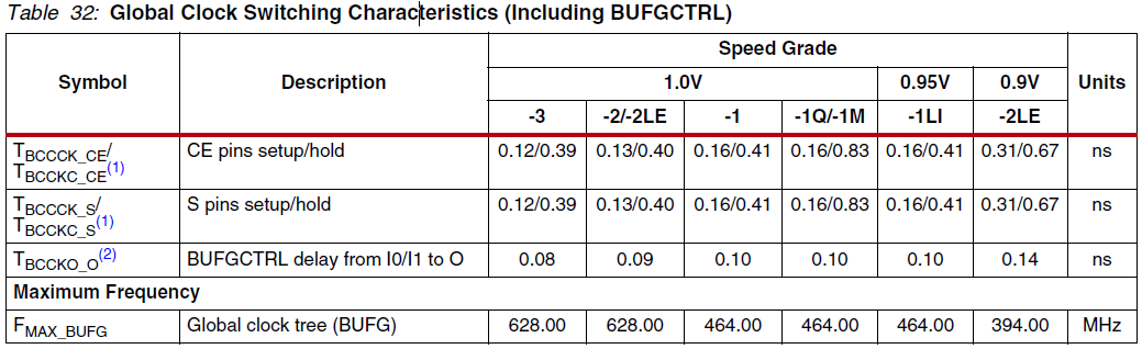
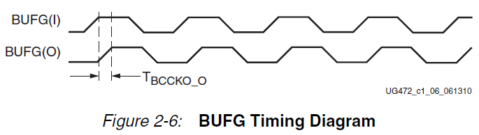
根据不同速度等级的芯片、这个延时不尽相同、大概在0.1ns左右。这里的Tbccko_o对应的就是UG472-Figure2-6中的BUFG的输入输出延时、如下图所示:
另外博文中还提到:
一些处理办法:用两个DCM级联来调相BUFG+DCM+DCM。
对应现在使用的7series FPGA中、也就是时钟BUFG+MMCM来实现时钟的相位调整。
关于DCM,MMCM和PLL的发展历史和区别,除了参阅UG472之外、在xilinx forum的回答下https://forums.xilinx.com/t5/Welcome-Join/DCM-MMCM-and-PLL/m-p/654372有详细说明:
The DCM is a Digital Clock Manager - at its heart it is a Delay Locked Loop. This has the ability to deskew a clock, generate different phases of the clock, dynamically change the phase of a clock, generate related (2x) clocks, do clock division, and even generate clocks with harmonic relationships to the incoming clock. It was the only clock management block that existed in older technologies (up to Spartan-3 and Virtex-4).
In Virtex-5 and Spartan-6 the Phase Locked Loop (PLL) was introduced along with the DCM. The PLL is an analog clock management cell that can do almost everything the DCM can do with the exception of dynamic and fine phase shifting. However, it can do more precise frequency generation and can generate multiple different frequencies at the same time. It also has significantly better jitter performance than the DCM - particularly when doing frequency synthesis with large multipliers/dividers.
In Virtex-6 the MMCM - Mixed Mode Clock Manager - was introduced. This is a PLL with some small part of a DCM tacked on to do fine phase shifting (that's why its mixed mode - the PLL is analog, but the phase shift is digital). Thus the MMCM can do everything the PLL can do plus the phase shifting from the DCM. The V6 only had MMCMs.
In the 7 series, they have a combination of PLLs and MMCMs. Mostly this is so that there are more cells available for use (the PLLs are smaller, so they take less room on the FPGA die). Furthermore the PLLs are tightly bound to the I/O structures that are used for DDRx-SDRAM memory controllers (via the MIG).
As for the number of them, that is determined by the size of the device. Look at the Product Table for the device you are using - it will tell you what is in the CMT (Clock Management Tile) and how many of them are available in your device.
转载于:https://www.cnblogs.com/lazypigwhy/p/11081972.html