table of Contents
Experimental explanations and exercises:
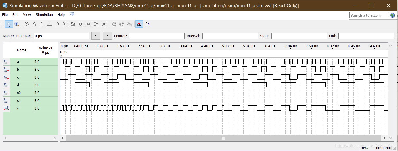
1. The source program of the multiplexer that chooses 1 from 4:
Experiment content: Digital display decoder design
7-segment digital display decoder source program:
7-segment digital display decoder simulation waveform:
Hardware verification of 7-segment digital display decoder:
Purpose:
1. Familiar with the use of QuartusⅡ software and master the EDA process;
2. Master the design methods of basic combinational logic circuits;
3. Learn the design of digital display decoder to lay the foundation for the design of complex digital systems.
Preview requirements:
1. Master the FPGA EDA design process (text input);
2. Master the basic structure of VerilogHDL programs, the use of always@procedure statements and case statements;
3. Master the design principles of digital display decoders.
Experimental explanations and exercises:
1. The source program of the multiplexer that chooses 1 from 4:
module mux41_a(a,b,c,d,s0,s1,y);
input a,b,c,d,s0,s1;

output y;
reg y;
always@ (*)
begin
	case ({s0,s1})
	2'b00:y<=a;
	2'b01:y<=b;
	2'b10:y<=c;
	2'b11:y<=d;
	default y<=a;
	endcase

end
endmodule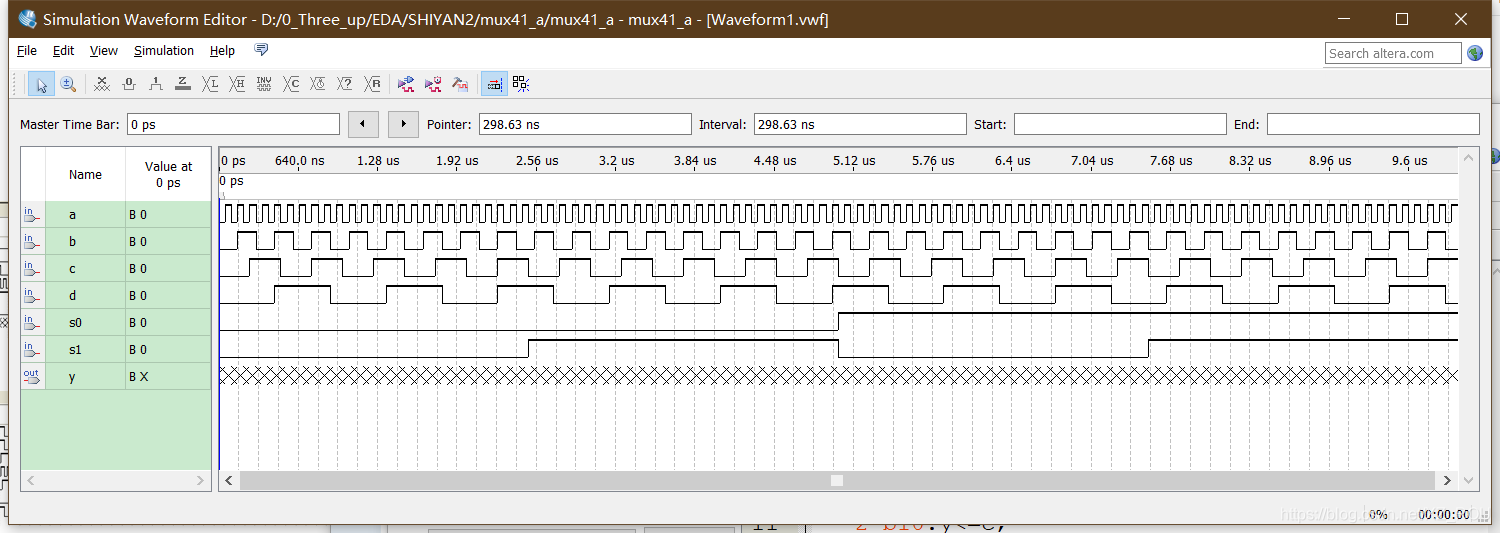
2. Grammar knowledge:
(1) Basic structure of VerilogHDL program:
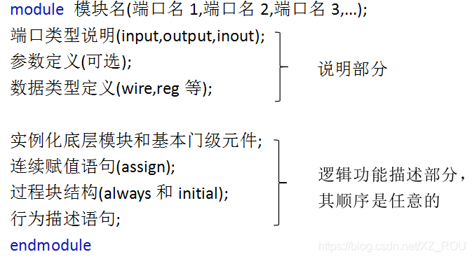
The program structure guided by the keyword module_endmodule of the Verilog language can completely express a circuit module or the port structure and function of an application-specific integrated circuit ASIC, that is, whether it is a 74LS138 or a CPU, it must be included in the module description statement module_endmodule .
Identifier: A string used to name objects (such as module names, circuit input and output ports, variables, etc.). The name can only contain the four symbols of English letters, numbers, underscores and $ ; note that it must start with English letters or underscores. For example, clk, counter8, _net, bus_A. Identifiers are case-sensitive, that is, the system is case sensitive.
Recommended program file name should as far as possible and consistent with the program's module name (for QuartusII , must meet this requirement), when the file name is case-sensitive, the file name should not be used to name the Chinese or digital, Verilog program must be saved to a file Folder (requires a non-Chinese folder name), do not exist in the root directory or on the desktop.
(2) always procedure statement
Syntax point 1: The procedural sentence structure guided by always@ is one of the most commonly used and important sentence structures in the Verilog language.
Syntax point 2: Sequential statement and parallel statement in Verilog?
Parallel statements: no matter how many lines of statements are executed at the same time, it has nothing to do with the order of the statements;
Sequential statement: Similar to the program execution method of ordinary software, it is executed in sequence according to the sequence of the statements.
Syntax point 3: The always procedure statement is a parallel statement, and any sequential statement must be placed in the procedure statement structure.
Syntax point 4: always procedure statement format:
always @( sensitive signal expression )
begin
// Procedure assignment statement ;
// if statement, case statement ;
// for statement, while statement, repeat statement ;
end
Syntax point 5: When any signal in the sensitive signal expression changes, the statement in the block will be executed once.
Grammar point 6: The expression of sensitive signals:
(a) Connect all sensitive signals with text or, expressed as always@(a or b or c or d or s0 or s1);
(b) Use commas to distinguish and connect all sensitive signals, expressed as always@(a,b,c,d,s0,s1);
(c) The omitted form is expressed as always@(*). The current mainstream Verilog synthesizers list all the signals that should be included in the default procedure statement. always@(*) conforms to the verilog HDL2001 specification, so it is invalid to try to change the logic design by selectively including sensitive signals.
(3) Block statement begin_end
The block statement begin_end itself has no function and is limited to use in the sequential statement structure. It is usually used to combine sequential statements, so it is called a sequential block. The block statement begin_end is only equivalent to a parenthesis, and the statements in the "brackets" are deemed to belong to the same operation module.
Verilog stipulates that if a statement structure contains only one statement and no local variables need to be defined, the block statement is used by default, and there is no need to explicitly define the block; if it contains multiple statements, you must use the explicit structure of begin_end to combine them. "Enclosed".
Block statement begin_end format:
begin [: block name ]
Statement 1 ; Statement 2 ; ... Statement n ;
end
Among them, [:block name] can be omitted.
(4) case statement
Syntax point 1: It is a multi-branch conditional selection statement, which is a sequential statement and must be used in a procedural statement.
Grammar point 2: There are three forms. Its general form is as follows:
case (case_expr)
item_expr1: begin statement1; end
item_expr2: begin statement2; end
……
default: begin default_statement; end
endcase
Syntax point 3: What does the Default statement mean?
Unless the selection value in all conditional statements can completely cover the value of the expression in the case statement, the default statement must be added to the selection in the last conditional statement.
It is recommended to add a default statement, because in Verilog, any variable has 4 different logic state values-0, 1, z and x, so the value of {S1, S0} is not only 00, 01, 10 And 11, if not added, some synthesizers will add unnecessary timing modules.
(5) Bit splicing operator {}
The function is to splice some bits of two or more signals into a new operand to perform arithmetic operations. Set A=1'b1, B=2'b10, C=2'b00
Then {B,C}=4'b1000
{A,B[1],C[0]}=3’b110
{A,B,C,3’b101}=8’b11000101。
Repeated splicing of the same operand can also use the operator formed by double curly braces { {}}
For example, {4{A}}=4'b1111, {2{A},2{B},C}=8'b11101000.
(6) Digital expression in Verilog
Represents the general format of a binary number
<bit width>'<base><number>
Bit width: the number of bits in the binary system of the data;
Base: Represents the base of the data, where B stands for binary, O stands for octal, D stands for decimal, H stands for hexadecimal, and is not case sensitive.
Example: 2'b10 4'b1011 4'hA 3'D7
Experiment content: Digital display decoder design
The data processing and operation in the digital system are both binary, so the output expressions are all hexadecimal; in order to meet the decoding and display of hexadecimal numbers, the most convenient way is to use the decoding program to implement in FPGA/CPLD .
The general decoding circuit is described by case sentences .
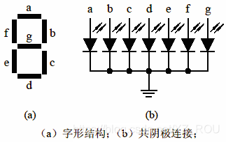
Design requirements: The input is a 4-digit binary number (that is, 0-15), and the output is a 7-digit binary number, which is used to light up the LED light and display the font from 0 to 15. Of course, 10 to 15 are represented by the letters A to F.

7-segment digital display decoder source program:
module decode_1(A, LEDS);
input[3:0] A;
output reg[6:0] LEDS;
always@ (A)
begin
	case (A)
	4'b0000:LEDS<=7'b0111111;	//"0"
	4'b0001:LEDS<=7'b0000110;	//"1"
	4'b0010:LEDS<=7'b1011011;	//"2"
	4'b0011:LEDS<=7'b1001111;	//"3”
	4'b0100:LEDS<=7'b1100110;	//"4"
	4'b0101:LEDS<=7'b1101101;	//"5"
	4'b0110:LEDS<=7'b1111101;	//"6"
	4'b0111:LEDS<=7'b0000111;	//"7"
	4'b1000:LEDS<=7'b1111111;	//"8"
	4'b1001:LEDS<=7'b1101111;	//"9"
	4'b1010:LEDS<=7'b1110111;	//"A"
	4'b1011:LEDS<=7'b1111100;	//"b"
	4'b1100:LEDS<=7'b0111001;	//"c"
	4'b1101:LEDS<=7'b1011110;	//"d"
	4'b1110:LEDS<=7'b1111001;	//"E"
	4'b1111:LEDS<=7'b1110001;	//"F"

	default:LEDS<=7'b0111111;	//"0"
	endcase

end
endmodule
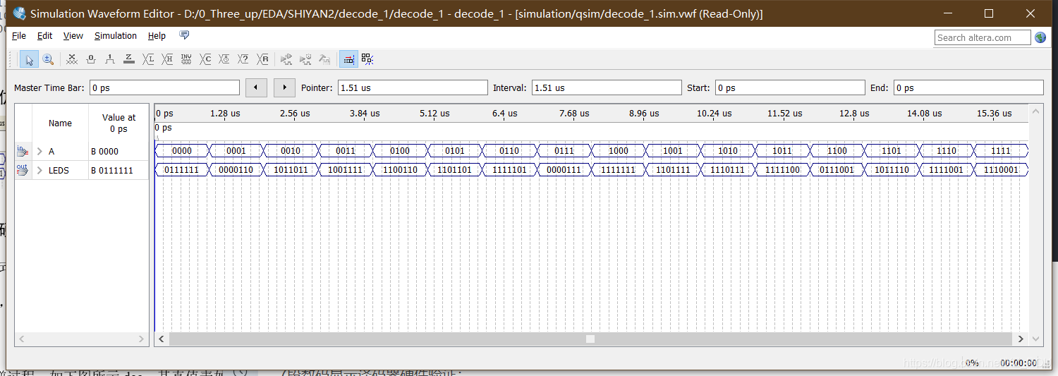
7-segment digital display decoder simulation waveform:
Hardware verification of 7-segment digital display decoder:
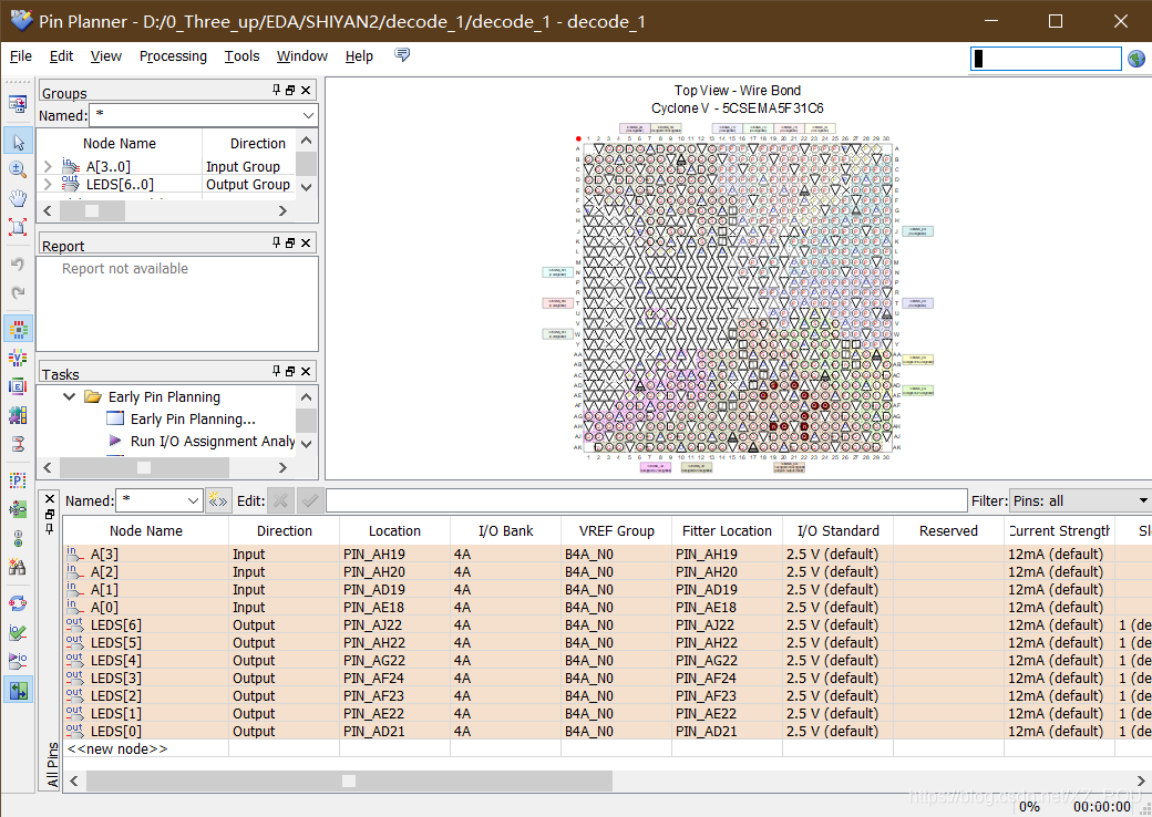
- It is recommended to choose experimental mode 6; [As for the method of mode selection, according to the needs of the circuit and the function of the mode]
- Schematic diagram of pin assignment [lock according to the corresponding pin manual of the mode] , where A[3:0] is the key input, and LEDS[6:0] is the seven-segment digital tube output.
Experiment summary