table of Contents
Custom LPM_ROM module process:
1. Customize the initialization data file and create a .mif format file
3. Build a project on the generated files, compile and simulate, and generate rom_1 components.
Option 1: Emulate ROM components
Elective 2: Simulation of the top-level design
The first method (using SignalTap II Logic Analyzer)
The second method: (simulation with Modelsim)
Purpose:
Be further familiar with Quartus II and the use of LPM_ROM and FPGA hardware resources.
Experiment preview:
Customize the LPM_ROM module process.
Experimental principle:
EDA is electronic design automation, the object is digital circuit design, but the design of sine signal generator is an analog circuit design, so a D/A converter is needed.
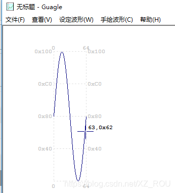
According to the waveform of the sine signal generator, it is known that the input of this experiment is time and the output is amplitude. If the amplitude of the sine wave on memory storage unit of the ROM 64 , according to the function that the ROM, data and address ROM is one relationship, so the design is converted by the corresponding relationship between the time and amplitude for the time and address The corresponding relationship. Accordingly, in order to obtain a sine signal, a 6-bit binary counter needs to be designed . The following figure shows the overall design block diagram:
In many practical situations, you must use megafunction modules to use the hardware functions of some Altera specific devices, such as various on-chip memories, DSP modules, and so on. These macro function blocks, which can be conveniently called in the form of graphics or hardware description language modules, have greatly improved the efficiency and reliability of electronic design based on EDA technology.
LPM is the English abbreviation for Library of Parameterized Modules. According to the design needs of the actual circuit, select the appropriate module in the LPM library and set appropriate parameters for it to meet your design needs, so that you can easily call the hardware of excellent electronic engineering technicians in your own projects. Design results.
The LPM function modules are rich in content. The functions, parameter meanings, usage methods, hardware description language module parameter settings and calling methods of each module can be found in the help in Quartus Ⅱ . The method is to select the help àMegafunction/LPM command.
Custom LPM_ROM module process:
1. Customize the initialization data file and create a .mif format file
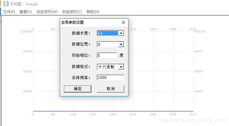
(1) Open the Mif arbitrary waveform editor Mif_Maker2010 [The software has uploaded the resource library] , select " Set Waveform"-"Global Parameters", modify the data length to 64 and the data width to 8 , as shown in Figure 1.
(2) Select " Set Waveform"-"Sine Wave", as shown in Figure 2.
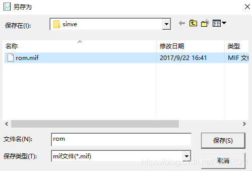
(3) Choose to save in the file and save it in the folder D:/myfile/sinve [It is recommended to save it in the directory of the project file to be used] . Note that sinve is the working library directory, as shown in Figure 3.
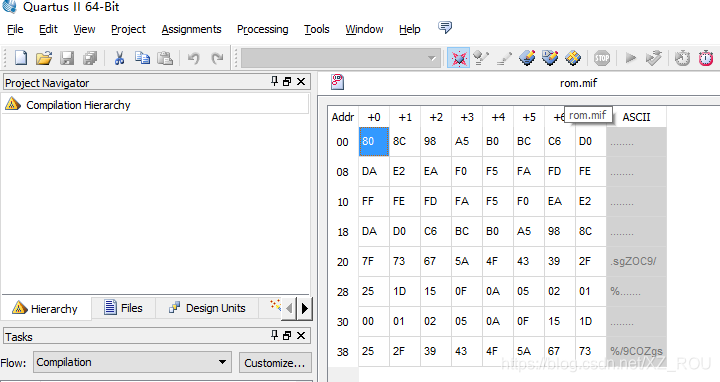
(4) Open the rom.mif file in the QuartusII software, as shown in Figure 4.
2. Custom LPM_ROM components
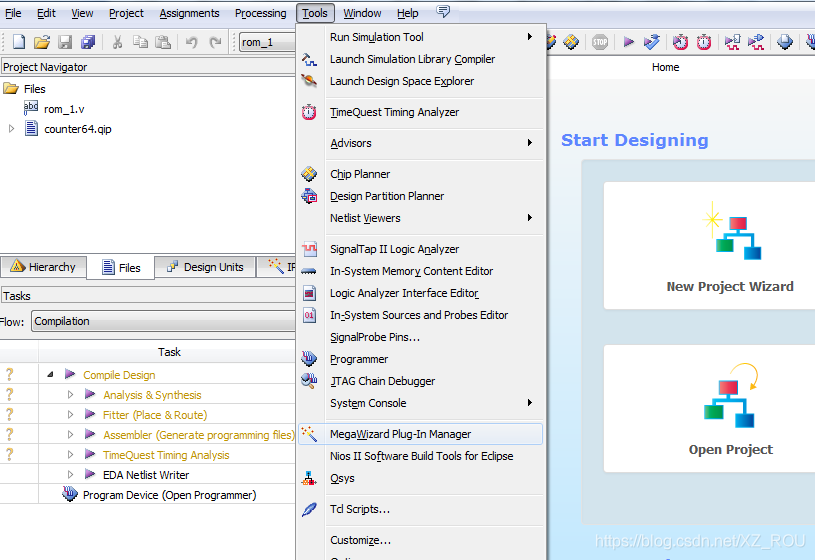
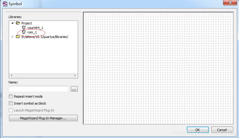
(1) Open the Tools menu and select "MegaWizard Plug-In Manager", as shown in Figure 5 below.
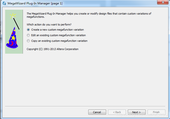
(2) Click to open the MegaWizard Plug-In Manager initial dialog box, and choose to create a new macro function module, as shown in Figure 6.
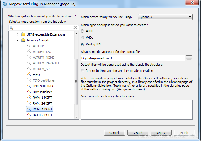
(3) Click "Next", select the macro function block (ROM: 1-PORT) , use device (ACEX1K ), output file information (file type: VerilogHDL; file address: D:\\myfile\sinve\; file name :Rom_1 ), as shown in Figure 7.
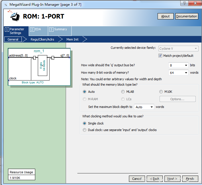
(4) Click "Next", select the ROM module to store the number of data bits and address line width (ie storage capacity) , as shown in Figure 8.
(5) Click on "Next", selected from the selection address latch signal inclock, as shown in FIG.
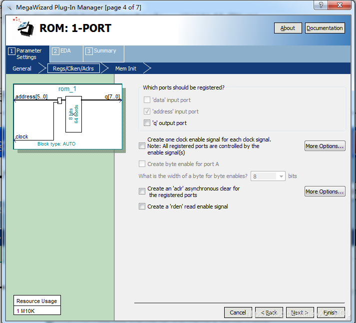
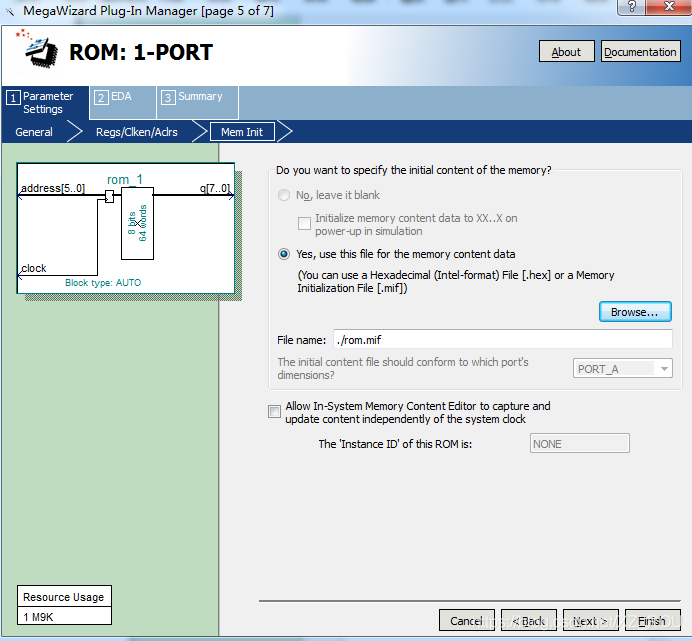
(6) Click "Next" to import the customized .mif file, [the most important step]
(7) The default simulation library, as shown in Figure 11, does not make any selections.

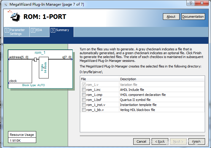
(8) Select the type of file to be generated, rom_1.v is generated by default, and you can freely choose to let the system generate more files. [It is recommended to tick all the last three boxes]
3. Build a project on the generated files, compile and simulate, and generate rom_1 components.
(1) First find the generated file rom_1.v in the folder D:\\myfile\sinve\;
(2) Set rom_1.v as the current project and compile it;
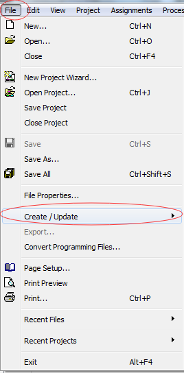
(3) Click File-Create/Update-Create Symbol Files for Current File to generate rom_1 components, as shown in Figure 13.
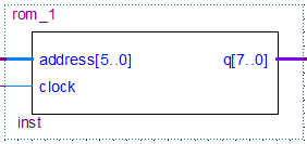
(4) Click File-New-BlcokDiagram/Schematic File, in the newly appeared interface, left-click and double-click, the following interface appears, double-click rom_1, the interface will appear rom_1 components.
Option 1: Emulate ROM components
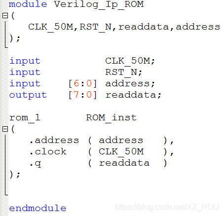
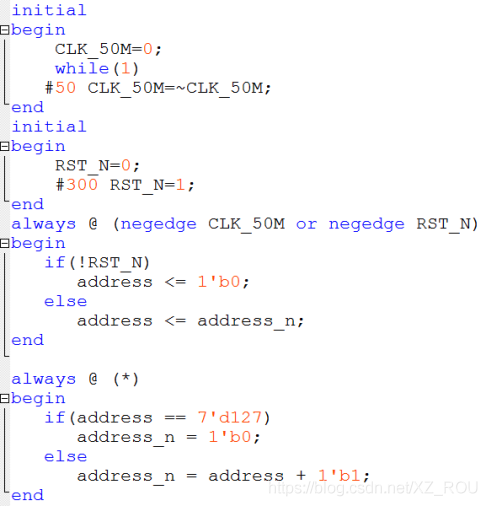
(1) Re-create a project, and its file source code is as shown in the figure below:
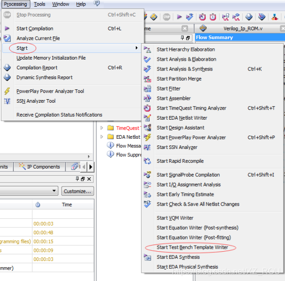
(2) Compile the project to generate a simulated test bench template. The generation method is to click Processing-Start-Start Test Bench Template Write, as shown in Figure 15 below.
(3) Open the sinve-simulation-modelsim folder, find the Verilog_Ip_ROM.vt file, and open it, as shown in Figure 16.

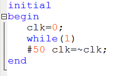
(4) Modify the initialization content of the test bench as shown below.
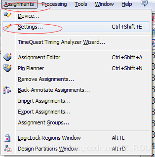
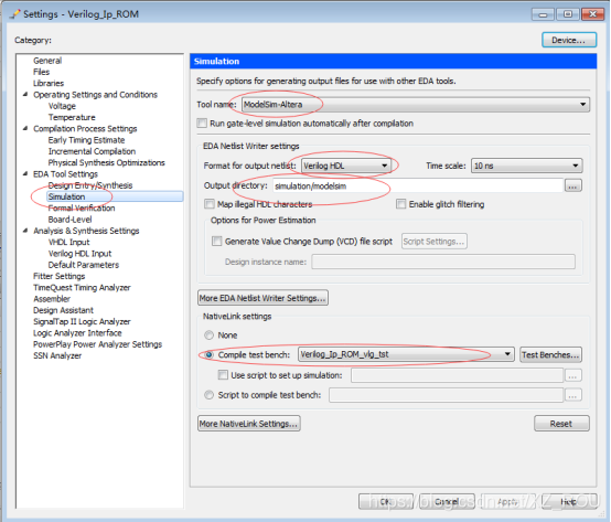
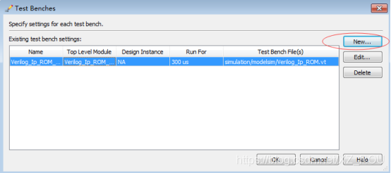
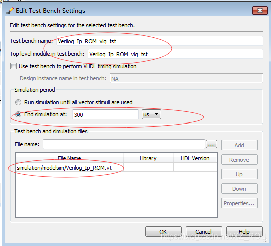
(5) Set the test bench, click Assignments-Settings-Simulation, select as shown in Figure 17, where the test bench name is the module name of the Verilog_Ip_ROM.vt file.
(6) Click Tools-Run Simulation Tool-RTL Simulation, as shown in the figure below, use Modelsim to simulate.

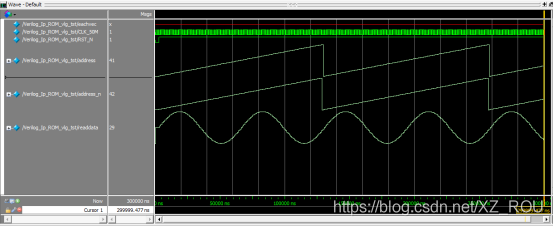
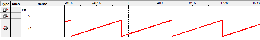
(7) The simulation result is shown in Figure 19. Note that right-click on the signal and select the display mode as
According to the custom LPM_ROM module process described above, complete the following experimental tasks.
Experiment task one
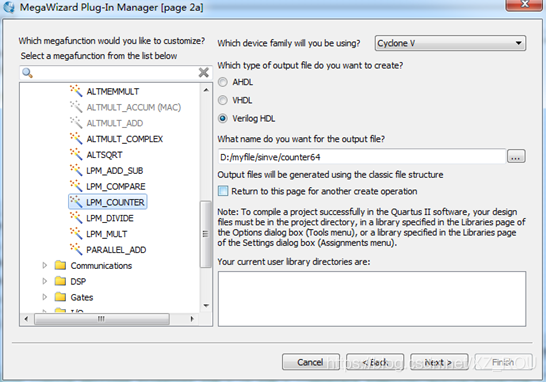
According to the usage method of the above QuartusⅡ megafunction module, select "LPM-COUNTER" in "Arithmetic" to design a 6-bit counter, build a project, compile and simulate the generated counter1.v file, and generate counter64 components.
Note: Selection of counter macro function block:
Experimental task two
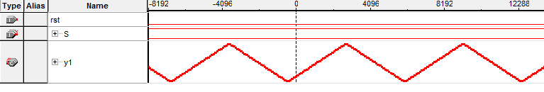
Complete the complete design of the sine signal generator, and give its timing waveform and analysis.

Elective 2: Simulation of the top-level design
The first method (using SignalTap II Logic Analyzer)
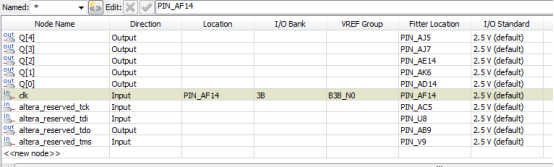
(1) Lock the clk pin to the system clock. The clock pin should be read from the user manual of Youjing. It is directly given here, which is AF14. Then compile the whole process.
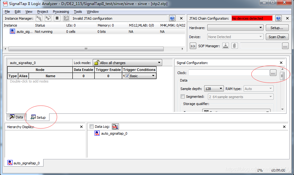
(2) Click File-New-signalTap II Logic Analyzer File, as shown in Figure 23.
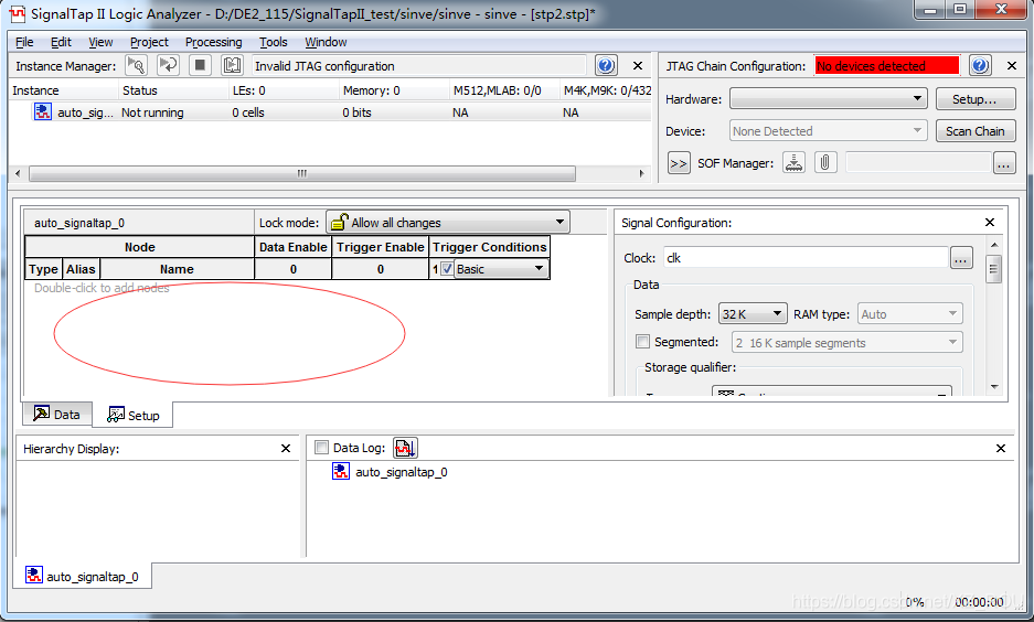
(3) In the pop-up interface, select setup and add the sampling clock clock, as shown in Figure 24 below.

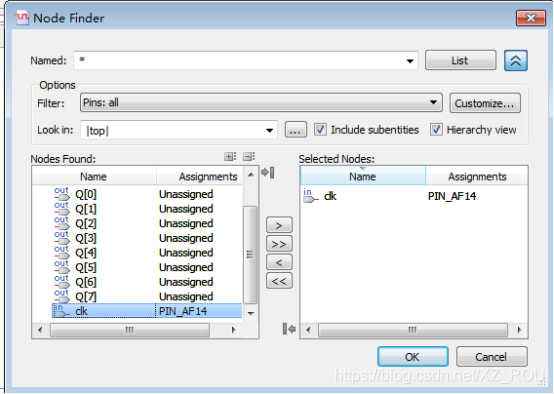
(4) Double-click to add output signal q[7:0] in the place as shown in the figure.
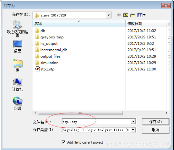
(5) Select File-Save As, enter the SignalTap II file name as stp1.stp (default file name and suffix), click the "Save" button, and a prompt will appear: "Do you want to enable SignalTap II.. ", you should click the "Yes" button to indicate that you agree to bundle this SignalTap II file with the project for synthesis/adaptation when compiling again, so that it can be downloaded into the FPGA chip to complete the real-time test task.
(6) Click the Processing-Start Compilation command to start the entire compilation.
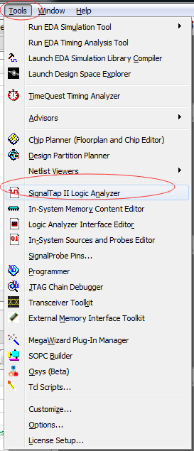
(7) Reopen, click Tools-SignalTap II Logic Analyzer, as shown in Figure 27.
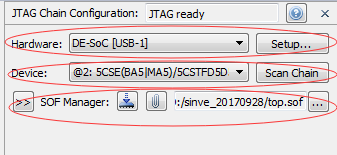
(8) Click the Setup button on the right to confirm the programmer mode, such as USB-Blaster. Then click the Scan Chain button beside the Device table box below to scan the development board. If the FPGA model name appears on the board, it means that the system JTAG communication is normal and you can download it. Press the "..." button, select the SOF file, click the download label on the left, and observe the download information in the lower left corner.
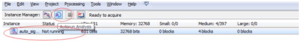
(9) Start SignalTap II for sampling and analysis, click the Instance name auto_sin, and then click the Autorun Analysis button in the Processing menu to start SignalTap II continuous sampling. The sampling waveform is shown in the figure below.
The second method: (simulation with Modelsim)
The process is the same as rom_1 simulation, the differences are listed as follows:
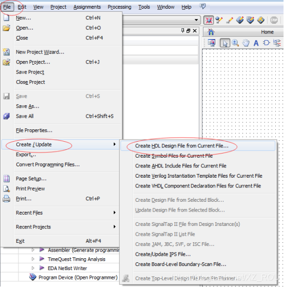
(1) Convert the top-level .bdf file into a .V file, as shown in Figure 30 below, click File-Create/Update-Create HDL Design File from Current File.
(2) After generating the test bench template, modify the initial content of the test bench as shown in the following code.
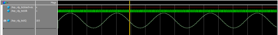
(3) The modelsim simulation waveform of the top-level design is shown in Figure 31.
Experiment task three
Hardware verification design of the function of the sinusoidal signal generator.
1 The experimental circuit mode can be selected
2 This experiment needs to use the DAC0832 expansion module, as shown in Figure 32. Note: If the expansion module is plugged into the main system for use, the +-12V socket of the main system should be selected, such as the experiment module 3 of our experiment box.

Among them: the mark "6" is the control terminal of DA0832, and the user can control it according to the 0832 manual. The label "7" is the data input terminal of the 0832 B channel. The label "8" is the data input terminal of channel A of the 0832. Marked "10, 12" are the A/B channel output connected to the oscilloscope port respectively. The labels "11, 13" are the positioners that adjust the amplitude of the A/B channel. In addition, there is a jumper cap on the left side of the 0832, which is a filter option, such as no filter when jumping down, and filtering when jumping up.
3 The 8-bit data port D[7..0] of DAC0832 can be connected to any 8 expansion ports of the 80-core port of FPGA, such as DB15~DB10 and DBT1, DBT0; the clock signal is connected to clockB0 of the system.
Assignment 1:
Design any of triangle waves, square waves, and sawtooth waves.
Tip: Just modify the data stored in ROM.
Assignment 2:
Design a signal generator that can generate triangle waves, square waves, sine waves and sawtooth waves.
Tip: Use the multiplexer.
Experiment summary and analysis