Purpose:
1. Learn to design an 8-bit multiplier by applying the shift-and-add principle.
2. Understand the advantages of the shift-and-add principle to form a multiplier and the circuit with the same function directly designed with a combinational logic circuit.
Design method:
Method 1: (Use multiplication sign to achieve multiplication)
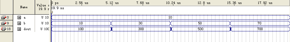
module chengfaqi(a,b,dout);
input [7:0] a,b;
output [15:0] dout;
assign dout=a*b;
endmodule
Simulation waveform:
Method 2: (Multiplication is achieved by shifting and adding)
module cfq_ywxj_1(a,b,dout);
input[7:0] a,b;
output reg[15:0] dout;
reg[7:0] a_buf,b_buf;
reg[3:0] i;
always@(*)
begin
	a_buf<=a;
	b_buf<=b;
	dout=0;
	for(i=0;i<8;i=i+1)
	if(a_buf[i]) dout=dout+(b_buf<<i);//移位相加逻辑
end
endmodule
Simulation waveform:

Experiment content
Main body (shift and add, sequential circuit)
explain
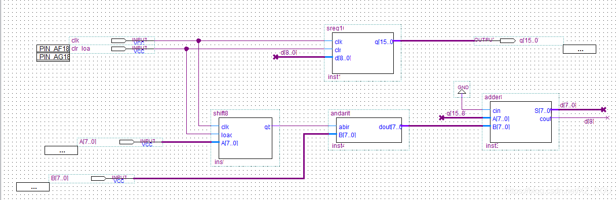
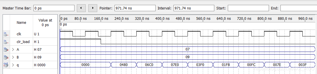
Multiplication can be realized by the principle of item-by-item shift and addition. For example, the first method is an 8-bit shift addition type multiplier based on the timing structure. Starting from the lowest bit of the multiplicand, if it is 1, the multiplier is shifted to the left and added to the previous sum; if it is 0, it is added to all 0s after shifting to the left until the highest bit of the multiplicand. The working principle of this multiplier can be clearly seen from the logic circuit diagram shown in FIG. 1 and the timing diagram of the multiplication operation. In order to better understand its working principle, no control circuit is added in Figure 1. In the shift timing waveform diagram, the rising edge of the LD signal has two functions, that is, the module sreg16 is cleared to 0 and the multiplicand A[7..0] is loaded to the shift register shift8; its low level is used as the multiplication enable signal. CLK is the clock signal. After the multiplicand is loaded into the 8-bit right shift register shift8, with each clock beat, the lowest bit is in the front, and it is shifted out from the low bit to the high bit one by one. When it is 1, the 1-bit multiplier andarith is turned on, and the 8-bit multiplier B[7..0] enters the 8-bit adder at the same beat, and is added to the upper 8 bits latched in sreg16 last time, and the sum is in the next The rising edge of the clock tick is latched into this latch. And when the shifted out bit of the multiplicand is 0, the addarith is all 0 output. So reciprocating, until after 8 clock pulses, the final product completely appears on the sreg16 port.
1-bit multiplier design
Design reason: Each bit of A needs to be multiplied by each bit of B
(1) After 7 clock cycles, the 8-bit shift register serially outputs each bit of A, from low to high sequentially
 always@(posedge clk or posedge load)
        begin
            if(load) reg8<=A;

          else reg8[6:0]<=reg8[7:1];
        end
        assign qb=reg8[0];
(2) A bit of A and each bit of B are multiplied, using a for loop statement
for(i=0;i<=7;i=i+4'b1)
dout[i]<=B[i]&abin;
Involving grammatical knowledge: loop statement (for statement)
The syntax format of the for statement:
for ( initial value setting expression; control condition expression; control variable value-added expression)
begin
loop body statement structure;
end
If the value of "control variable value-added expression" does not change with the loop, or the number of loops is too large, for synthesis All will lead to design failure.
3) Shift and add
(1) 16-bit shift register The high bit shifts to the left in turn means that the low bit is shifted to the high bit to the right in turn
Compared with the product of A[i]*B, the product of A[i-1]*B is shifted one bit to the right.
reg16[6:0]<=reg16[7:1];
q[15:7]<=d[8:0]
(2) 8-bit binary adder
A[i-1]*B+ A[i]*B
(For A[i-1]*B, shift 1 bit to the right and add A[i]*B)
d[8:0]<=q[ 15:8]+B[7:0]
Each part of the module:
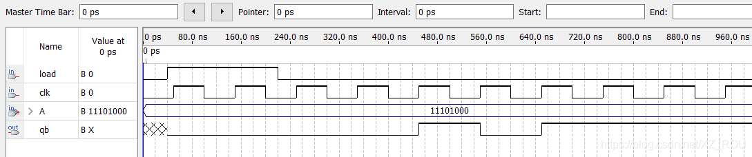
1) 8-bit shift register
module shift8(clk,load,A,qb);			//8位移位寄存器
input clk,load;							//输入时钟、载路信号
input[7:0] A;								//输入8位二进制数值A
output qb;									//输出
reg[7:0] reg8;								//8位二进制寄存器
always@(posedge clk or posedge load)//	检测敏感信号,时钟信号上升沿或载路信号上升沿
begin
	if(load) reg8<=A;						//如果载路信号为1,则将A值赋给寄存器reg8
	else reg8[6:0]<=reg8[7:1];			//否则,将reg8中的数据向右移一位
end
assign qb=reg8[0];						//将寄存器中的最低位,赋给qb进行输出
endmodule									//模块结束
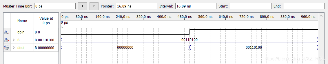
2) 1-bit multiplier
module andarith(abin,B,dout);//1位乘法器,与门
input abin;
input[7:0] B;
output reg[7:0] dout;
reg[3:0] i;
always@(*)
begin
	for(i=0;i<=7;i=i+4'b1)
	dout[i]<=B[i]&abin;
end
endmodule
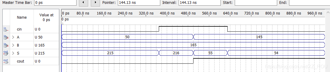
3) 8-bit adder
module adder8(cin,A,B,S,cout);//8位加法器
input cin;
input[7:0] A,B;
output[7:0] S;
output cout;
assign {cout,S}=cin+A+B;
endmodule
4) 16 bit shift register
module sreg16(clk,clr,d,q);			//16位移位寄存器
input clk,clr;								//输入时钟和复位信号
input[8:0] d;								//输出9位二进制数值
output[15:0] q;							//输出16位二进制数值
reg[15:0] reg16;							//16位二进制寄存器
always@(posedge clk or posedge clr) //时钟和复位信号的上升沿有效
begin
	if(clr)  reg16<=16'b0;				//如果复位信号为1,则将寄存器内容全部清零
	else
	begin reg16[6:0]<=reg16[7:1];		//否则,向右移1位
			reg16[15:7]<=d;				//将输入的值,赋给寄存器的高9位
	end
end
assign q=reg16;							//输出寄存器中的值
endmodule									//模块结束

Dig:
5) Controller
module arictl(clk,start,ariend,clkout,rstall,cnt4);
input clk,start;
output reg ariend,clkout;
output rstall;
output reg[3:0] cnt4;
always@(posedge clk or posedge start)
begin
		if(start) cnt4<=4'b0;
		else if(cnt4<4'b1000) cnt4<=cnt4+4'b1;
end
always@(*)
begin
	if(~start)
		if((cnt4<4'b1000)&(cnt4>=4'b0001)) begin clkout<=clk;ariend<=1'b0;end
		else if(cnt4==4'b0000) begin clkout<=1'b0;ariend<=1'b0;end
		else begin clkout<=1'b1;ariend<=1'b1;end
		else begin clkout<=1'b0;ariend<=1'b0;end
end
assign rstall=start;
endmodule

Summary and analysis: