After the transfer of DDR3 IP core, is not directly read and write tests, you must first perform an initialization operation, check IP core. Benpian using Modelsim software with the simulation model DDR3 IP core generation, build the initialization process IP core.
A top-level documents
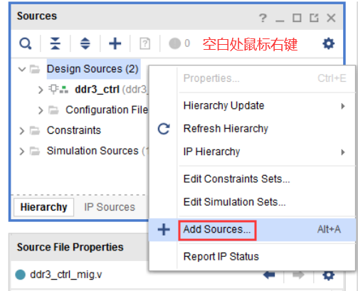
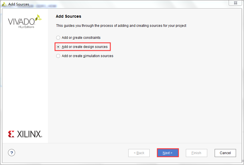
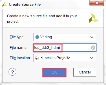
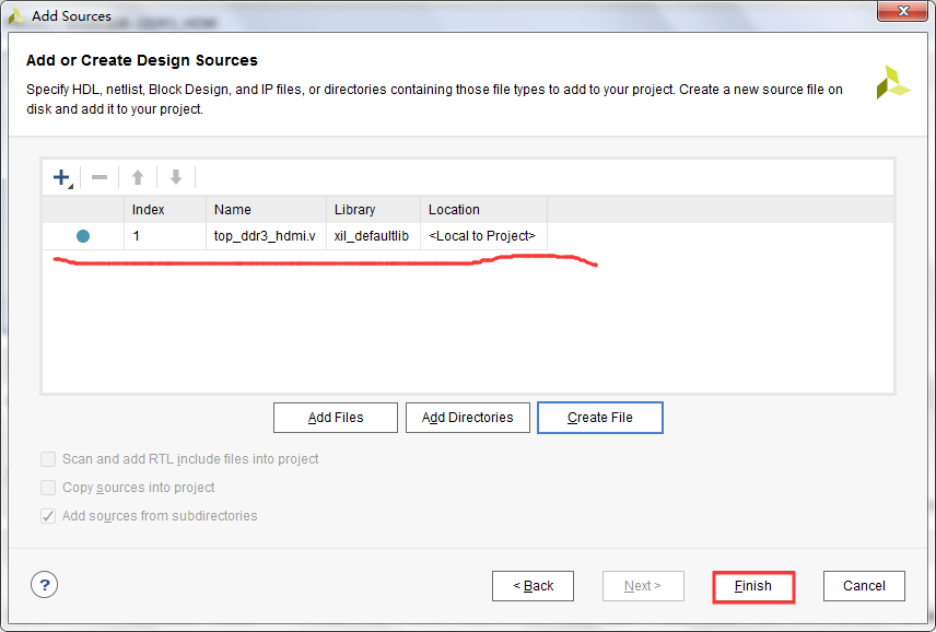
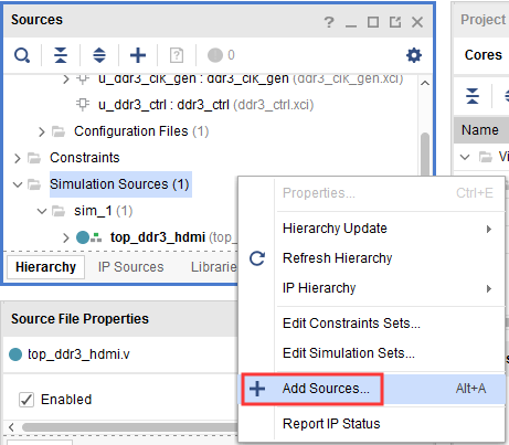
1, after generation DDR3 IP core, right-click on the Source screen blank Add Source, add a top-level file.

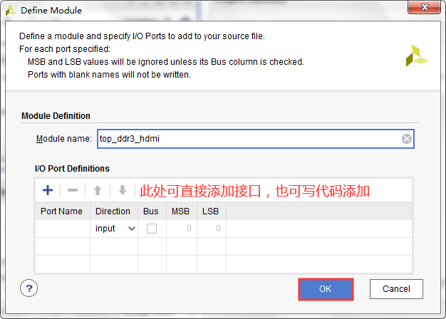

2, the DDR3_HDMI \ DDR3_HDMI.srcs \ sources_1 \ ip \ ddr3_ctrl \ ddr3_ctrl \ user_design \ rtl \ ddr3_ctrl.v available input and output ports top_ddr3_hdmi need to copy it over.
 1 module top_ddr3_hdmi
 2 //========================< 端口 >==========================================
 3 (
 4 // inout ----------------------------------------
 5 inout   wire  [15:0]        ddr3_dq             ,
 6 inout   wire  [ 1:0]        ddr3_dqs_n          ,
 7 inout   wire  [ 1:0]        ddr3_dqs_p          ,
 8 // output ---------------------------------------
 9 output  wire  [13:0]        ddr3_addr           ,
10 output  wire  [ 2:0]        ddr3_ba             ,
11 output  wire                ddr3_ras_n          ,
12 output  wire                ddr3_cas_n          ,
13 output  wire                ddr3_we_n           ,
14 output  wire                ddr3_reset_n        ,
15 output  wire  [ 0:0]        ddr3_ck_p           ,
16 output  wire  [ 0:0]        ddr3_ck_n           ,
17 output  wire  [ 0:0]        ddr3_cke            ,
18 output  wire  [ 0:0]        ddr3_cs_n           ,
19 output  wire  [ 1:0]        ddr3_dm             ,
20 output  wire  [ 0:0]        ddr3_odt            ,
21 // system ---------------------------------------
22 input   wire                sclkin              ,
23 input   wire                srst_n
24 );
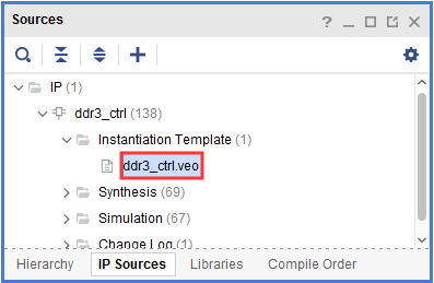
3, the top-level module to write, you can enter the IP Source of ddr3_ctrl.veo found files copied example of the interface, and change the part of the signal according to demand.

 1 ddr3_ctrl u_ddr3_ctrl
 2 (
 3     // Memory interface ports -----------------------
 4     .ddr3_addr              (ddr3_addr              ),  // output [13:0]    ddr3_addr
 5     .ddr3_ba                (ddr3_ba                ),  // output [2:0]     ddr3_ba
 6     .ddr3_cas_n             (ddr3_cas_n             ),  // output           ddr3_cas_n
 7     .ddr3_ck_n              (ddr3_ck_n              ),  // output [0:0]     ddr3_ck_n
 8     .ddr3_ck_p              (ddr3_ck_p              ),  // output [0:0]     ddr3_ck_p
 9     .ddr3_cke               (ddr3_cke               ),  // output [0:0]     ddr3_cke
10     .ddr3_ras_n             (ddr3_ras_n             ),  // output           ddr3_ras_n
11     .ddr3_reset_n           (ddr3_reset_n           ),  // output           ddr3_reset_n
12     .ddr3_we_n              (ddr3_we_n              ),  // output           ddr3_we_n
13     .ddr3_dq                (ddr3_dq                ),  // inout [15:0]     ddr3_dq
14     .ddr3_dqs_n             (ddr3_dqs_n             ),  // inout [1:0]      ddr3_dqs_n
15     .ddr3_dqs_p             (ddr3_dqs_p             ),  // inout [1:0]      ddr3_dqs_p
16     .init_calib_complete    (init_calib_complete    ),  // output           init_calib_complete
17     .ddr3_cs_n              (ddr3_cs_n              ),  // output [0:0]     ddr3_cs_n
18     .ddr3_dm                (ddr3_dm                ),  // output [1:0]     ddr3_dm
19     .ddr3_odt               (ddr3_odt               ),  // output [0:0]     ddr3_odt
20     // Application interface ports ------------------
21     .app_addr               (app_addr               ),  // input [27:0]     app_addr
22     .app_cmd                (app_cmd                ),  // input [2:0]      app_cmd
23     .app_en                 (1'b0                   ),  // input            app_en
24     .app_wdf_data           (app_wdf_data           ),  // input [127:0]    app_wdf_data
25     .app_wdf_end            (1'b0                   ),  // input            app_wdf_end
26     .app_wdf_wren           (1'b0                   ),  // input            app_wdf_wren
27     .app_rd_data            (app_rd_data            ),  // output [127:0]   app_rd_data
28     .app_rd_data_end        (app_rd_data_end        ),  // output           app_rd_data_end
29     .app_rd_data_valid      (app_rd_data_valid      ),  // output           app_rd_data_valid
30     .app_rdy                (app_rdy                ),  // output           app_rdy
31     .app_wdf_rdy            (app_wdf_rdy            ),  // output           app_wdf_rdy
32     .app_sr_req             (1'b0                   ),  // input            app_sr_req
33     .app_ref_req            (1'b0                   ),  // input            app_ref_req
34     .app_zq_req             (1'b0                   ),  // input            app_zq_req
35     .app_sr_active          (app_sr_active          ),  // output           app_sr_active
36     .app_ref_ack            (app_ref_ack            ),  // output           app_ref_ack
37     .app_zq_ack             (app_zq_ack             ),  // output           app_zq_ack
38     .ui_clk                 (ui_clk                 ),  // output           ui_clk
39     .ui_clk_sync_rst        (ui_clk_sync_rst        ),  // output           ui_clk_sync_rst
40     .app_wdf_mask           (app_wdf_mask           ),  // input [15:0]     app_wdf_mask
41     // System Clock Ports ---------------------------
42     .sys_clk_i              (sysclk                 ),  // input            sys_clk_i 200Mhz
43     .sys_rst                (srst_n                 )   // input            sys_rst
44 );
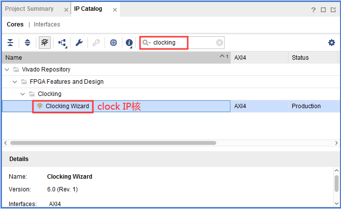
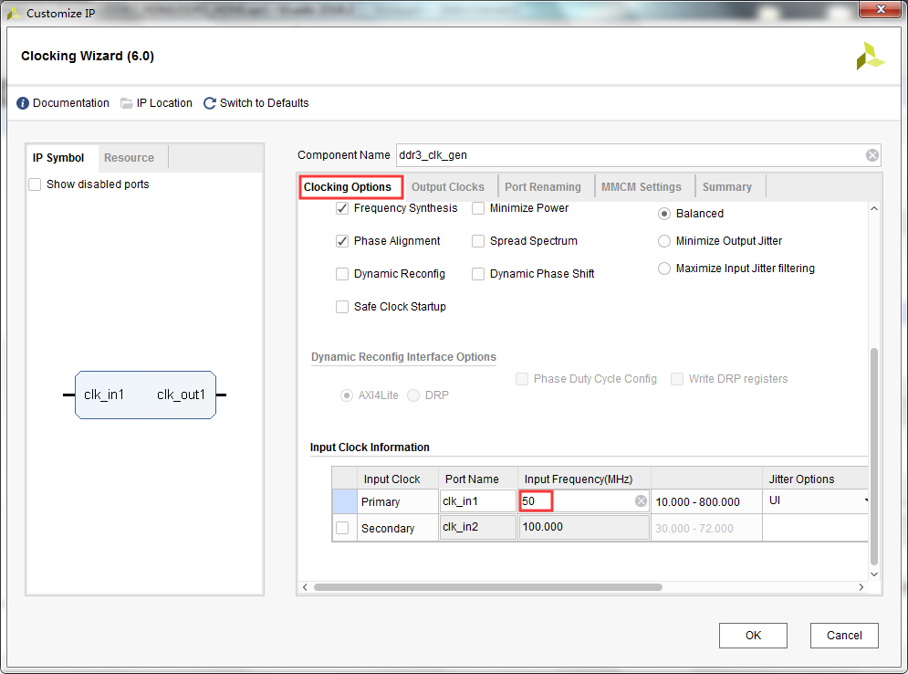
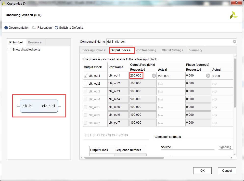
4, when the transfer of DDR3 IP core, IP core selected for this input a 200 Mhz clock, since the board 50Mhz crystal clock is generated, so have to use one IP core 200 Mhz clock birth.
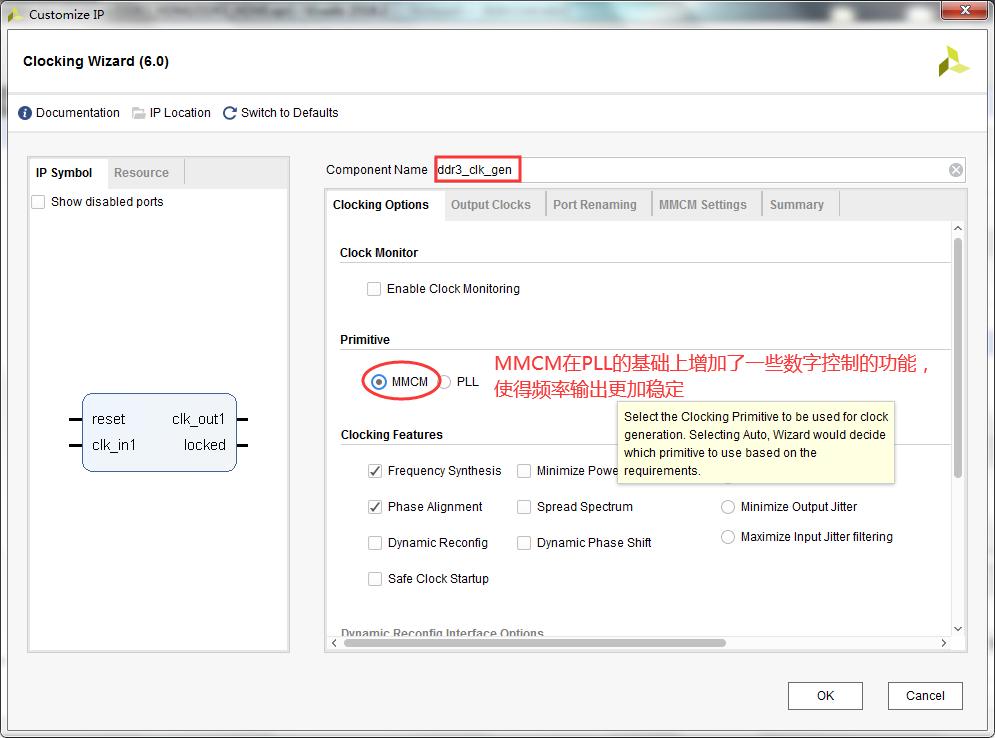
5, after generating the same clock to find .veo embodiment of the copied file interface.

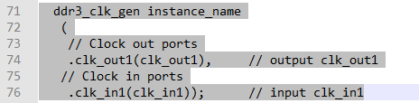
1 ddr3_clk_gen u_ddr3_clk_gen
2 (
3     .clk_out1               (sysclk                 ),  // output           clk_out1
4     .clk_in1                (sclkin                 )   // input            clk_in1
5 );
7, there are a few signals that we need to observe, by wire leads come.
1 //========================< 连线 >==========================================
2 wire                        sysclk              ;
3 wire                        init_calib_complete ;
4 wire                        ui_clk              ;
5 wire                        ui_clk_sync_rst     ;
Second, the test file
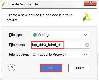
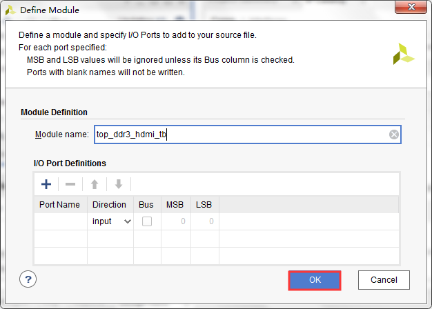
1, select Add Sources in the Simulation Sources Right, create testbench file.

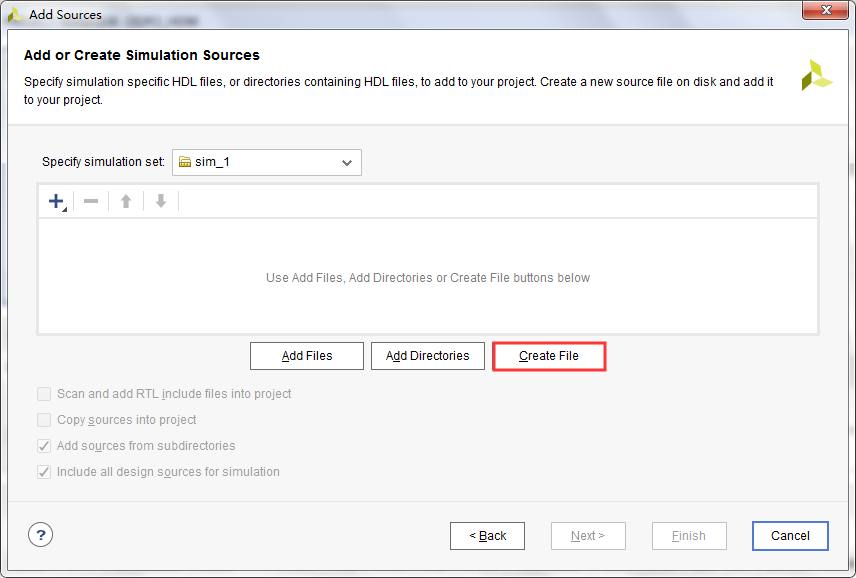

2, DDR3 controller is very complex, handwriting testbench is very difficult. When we talk about the transfer of a DDR3 IP core have said, it has generated a simulation model for us to test. Position in DDR3_HDMI \ DDR3_HDMI.srcs \ sources_1 \ ip \ ddr3_ctrl \ ddr3_ctrl \ example_design \ sim, ddr3_model.sv and ddr3_model_parameters.vh simulation model that is we need to interface testbench in cases of over.
 1 ddr3_model u_ddr3_model
 2 (
 3     .rst_n                  (ddr3_reset_n                   ),
 4     .ck                     (ddr3_ck_p                      ),
 5     .ck_n                   (ddr3_ck_n                      ),
 6     .cke                    (ddr3_cke                       ),
 7     .cs_n                   (ddr3_cs_n                      ),
 8     .ras_n                  (ddr3_ras_n                     ),
 9     .cas_n                  (ddr3_cas_n                     ),
10     .we_n                   (ddr3_we_n                      ),
11     .dm_tdqs (ddr3_dm {[ 1 ], ddr3_dm [ 0 ]}),
 12      .ba (ddr3_ba),
 13      .addr (ddr3_addr),
 14      .dq (ddr3_dq [ 15 : 0 ]),
 15      .dqs (ddr3_dqs_p {[ 1 ], ddr3_dqs_p [ 0 ]}),
 16      .dqs_n (ddr3_dqs_n {[ 1 ], ddr3_dqs_n [ 0 ]}),
 17      .tdqs_n (),
 18     .odt (ddr3_odt)
 19 );
3, also required a 50 Mhz clock and generates an active-low reset signal.
1  // =============================================== ===========================
 2  // == clock signal and a reset signal
 3  // ============== ================================================== ==============
. 4  Initial  the begin
. 5      CLK = 0 ;
 . 6      Forever
. 7          # ( `Clock / 2 ) = ~ CLK CLK;
 . 8  End
. 9
10  Initial  the begin
. 11      RST_N = 0 ; # ( Clock * ` 20 is + . 1 );
 12 is      RST_N = . 1 ;
13  End
4, back Vivado, found the simulation model file there have been, but the question mark in the state, we select it, right Add Sources, adding ddr3_model.sv and ddr3_model_parameters.vh to come.
Third, start Modelsim validate DDR3 IP core
1, before using Modelsim simulation, you need to compile the library association between Vivado and Modelsim, the procedure in a separate search.
2, click the Setting Vivado set, Target simulator choose ModelSim Simulator, the second step of the simulation top-level file selection simulation files, simulation library is automatically positioned better.
3. Click Vivado left menu Run Simulation --- Run Behavioral Simulation, Modelsim simulation will automatically open up.
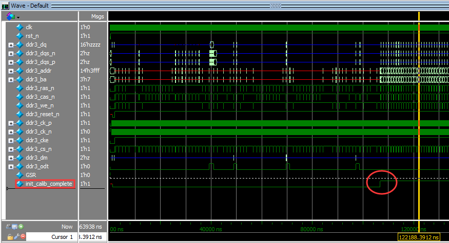
4, the selection signal, run time, you can see the clock signal and a reset signal is normal, init_calib_complete signal is pulled down after a period of time, the surface of this core DDR3 IP authentication is successful.
the above.
Reference: Wei-three FPGA Tutorial College