Table of contents
1 Introduction
PCIE (PCI Express) adopts the current popular point-to-point serial connection in the industry. Compared with the shared parallel architecture of PCI and earlier computer buses, each device has its own dedicated connection. It does not need to request bandwidth from the entire bus, and it can Improving the data transmission rate to a very high frequency and achieving the high bandwidth that PCI cannot provide is the preferred direction of high-speed interfaces in various industries at present, and has high practical value and learning value;
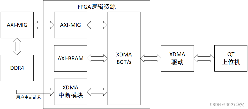
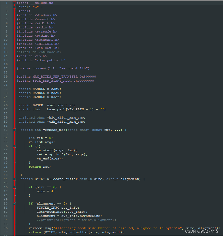
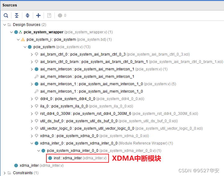
This design uses Xilinx's official XDMA solution to build a PCIE3.0 communication platform based on Xilinx series FPGAs, and uses the XDMA interrupt mode to communicate with the QT host computer, that is, the QT host computer implements data interaction with the FPGA through software interrupts; The key is that we have written an XDMA interrupt module of xdma_inter.v. This module is used to cooperate with the driver to handle interrupts. xdma_inter.v provides an AXI-LITE interface. The host computer reads and writes the registers of xdma_inter.v by accessing the user space address. The module registers the interrupt bit number in the interrupt bit input by user_irq_req_i, and outputs it to XDMA IP. When the driver of the upper computer responds to the interrupt, write the xdma_inter.v register in the interrupt to clear the processed interrupt. In addition, in this program, AXI-BRAM is used to demonstrate the read and write access test of the user space.
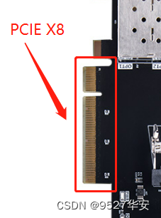
This solution is only applicable to Xilinx series FPGAs. It also provides the XDMA installation driver and QT host computer source code, which saves the trouble of using XDMA to find the tedious driver and the host computer software development, and to build a vivado project. It saves the embarrassment of not knowing how to use XDMA, making the use of PCIE easy to use, without worrying about its complicated PCIE protocol; since my development board only supports PCIE X8, the code provided is the PCIE X8 architecture. Friends who need PCIE X1, X2, X8, X16, X32 can modify this project by themselves, or follow me, I will release new projects in real time.
This project realizes the basic PCIE communication, and conducts a speed test with the QT host computer.
This article describes in detail the design scheme of building a PCIE communication platform based on XDMA. The engineering code can be comprehensively compiled and debugged on the board, and can be directly transplanted. High-speed interface fields in medical, military and other industries;
provide complete and smooth engineering source code and technical support;
the method of obtaining engineering source code and technical support is at the end of the article, please be patient to the end;
2. My existing PCIE solution
My homepage has a PCIE communication column, which implements data interaction with the QT host computer based on the polling mode of XDMA. There are both PCIE solutions based on RIFFA and PCIE solutions based on XDMA; both simple data interaction and speed measurement , there is also application-level image acquisition and transmission, the following is the column address:
click to go directly
In addition, my homepage has a PCIE communication column in interrupt mode, which realizes data interaction with the QT host computer based on the XDMA interrupt mode, the following is the column address : Click to go directly to
3. PCIE theory
For this part, you can learn theoretical knowledge from Baidu or csdn or Zhihu. In fact, XDMA is used, and there is no need for complex protocols and theories until PCIE. . .
4. Overall design idea and scheme
The overall design idea and scheme are as follows:
Introduction to XDMA
The DMASubsystem for PCIExpressIP provided by Xilinx is a high-performance, configurable SG mode DMA suitable for PCIE2.0 and PCIE3.0, providing user-selectable AXI4 interface or AXI4-Stream interface. Generally, the AXI4 interface can be added to the system bus interconnection, which is suitable for asynchronous transmission of large amounts of data. Usually, DDR is used, and the AXI4-Stream interface is suitable for low-latency data stream transmission.
XDMA is SGDMA, not Block DMA. In SG mode, the host will form the data to be transmitted in the form of a linked list, and then send the first address of the linked list to XDMA through BAR. XDMA will complete the transmission tasks specified by the linked list in turn according to the first address of the linked list structure. , the XDMA block diagram is as follows:
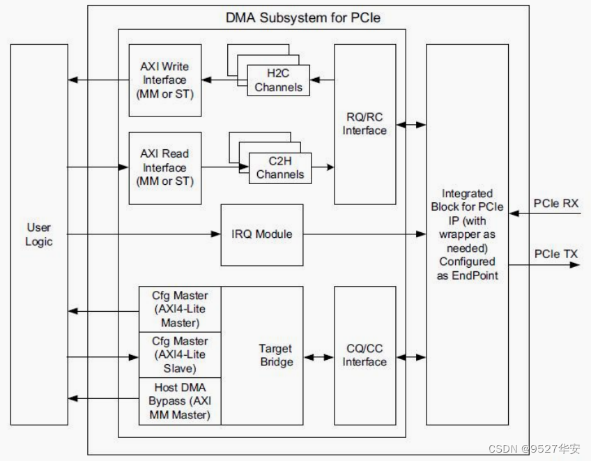
AXI4, AXI4-Stream, one must be selected for data transmission AXI4-Lite Master is optional, used to realize the mapping from PCIE BAR address to AXI4-lite register address, and can be used to read and write user logic registers.
AXI4-Lite Slave is optional and is used to open the XDMA internal registers to user logic. User logic can access XDMA internal registers through this interface and will not be mapped to BAR.
AXI4 Bypass interface, optional, used to implement PCIE pass-through user logic access, which can be used for low-latency data transmission.
XDMA interrupt mode
The key to this design is that we have written an XDMA interrupt module of xdma_inter.v. This module is used to cooperate with the driver to handle interrupts. xdma_inter.v provides an AXI-LITE interface. The host computer reads and writes the registers of xdma_inter.v by accessing the user space address. The module registers the interrupt bit number in the interrupt bit input by user_irq_req_i, and outputs it to XDMA IP. When the driver of the upper computer responds to the interrupt, write the xdma_inter.v register in the interrupt to clear the processed interrupt.
In addition, in this program, AXI-BRAM is used to demonstrate the read and write access test of the user space.
QT host computer and its source code
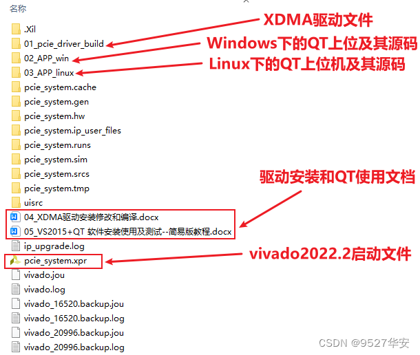
QT host computer This program uses VS2015 + Qt 5.12.10 to complete the development software environment of the host computer. The QT program calls the official XDMA API to realize data interaction with the FPGA in interrupt mode. This routine implements reading and writing speed measurement and provides QT host computer The path of the software and its source code is as follows:
The screenshot of QT source code is as follows:
5. Detailed explanation of vivado project
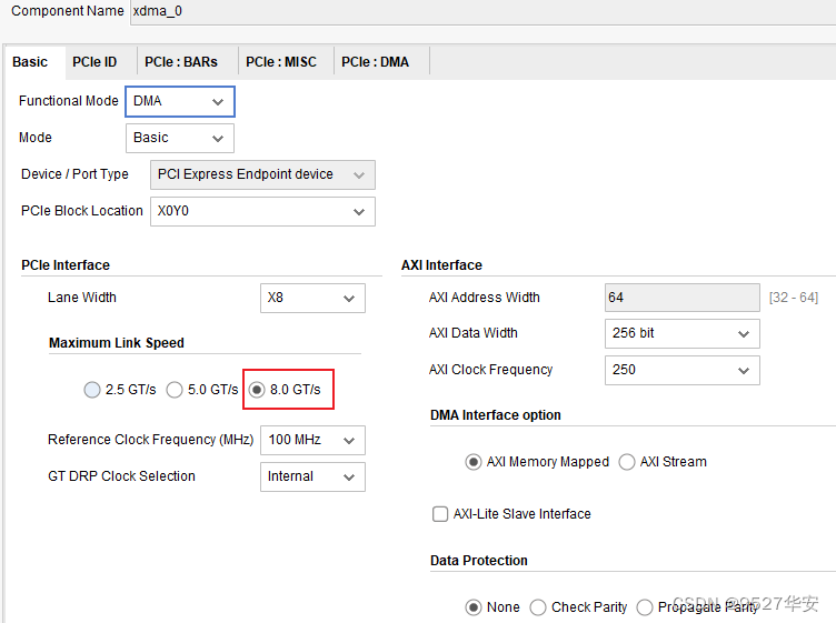
Development board FPGA model: Xilinx–xcku060-ffva1156-2-i;
development environment: Vivado2022.2;
input\output: PCIE3.0 X8;
application: QT host computer speed test;
project BD is as follows:

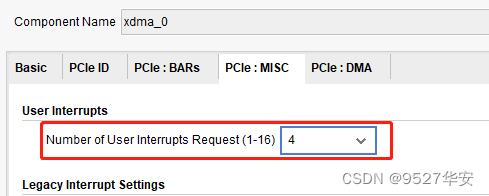
XDMA needs to design the number of interrupts, and the configuration is as follows:
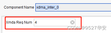
At the same time, the number of interrupts of the XDMA interrupt module is also set to 4, as follows:
The code structure after synthesis is as follows:
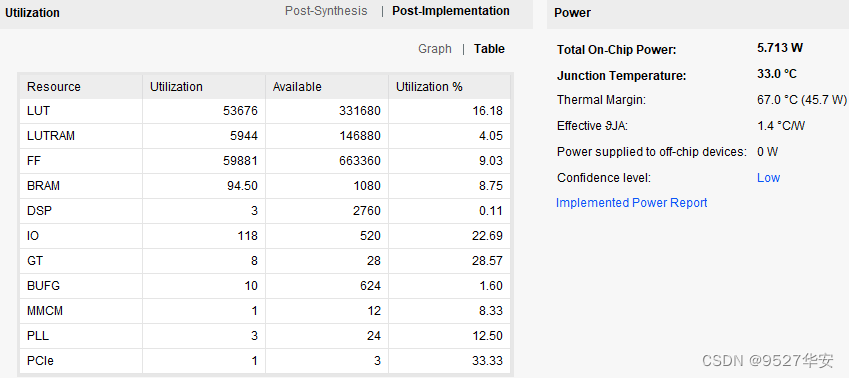
the FPGA resource consumption and power consumption after the synthesis is compiled are estimated as follows:
6. Board debugging and verification
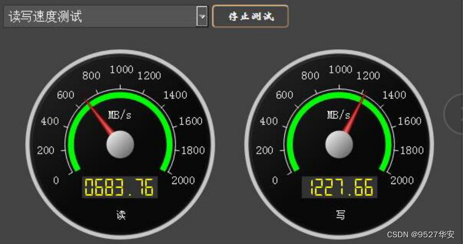
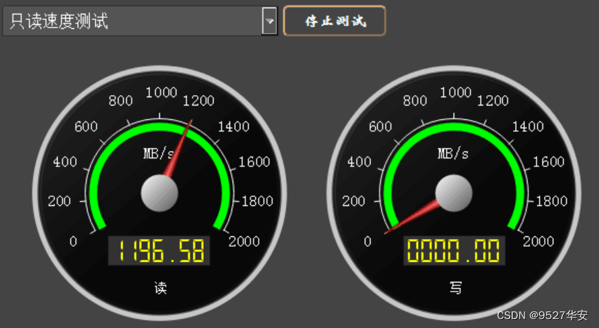
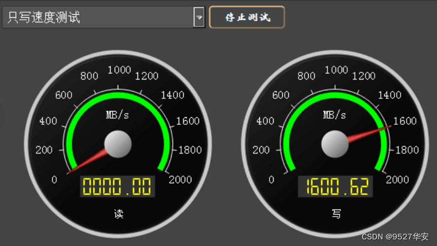
Open the host computer test program to test the PCIe speed, open the QT software, the experimental results are as follows:
read and write at the same time test:
read-only test:
write-only test:
7. Welfare: acquisition of engineering code
Benefits: Obtaining the engineering code
The code is too large to be sent by email, and it is sent by a certain degree network disk link. The
method of data acquisition: private, or the V business card at the end of the article.
The network disk information is as follows: