前言
- 之前刷过HDLbits上面的题目,点击链接可以查看详细笔记:verilog练习:hdlbits网站系列完结!
- 最近又想刷一下牛客上面的题目,可以点击链接与小编一起刷题:牛客刷题
- 小编不才,文中如有不当之处,可以在评论中互相交流。此处题目推荐看牛客的评论区,再提一嘴,注意积累自己的基本功
算法、设计模式、软件等
Part I Verilog快速入门
01. 基础语法
VL1 四选一多路器
答案
- 一个注意点: 自测运行时需要自己写testbench。第一次运行的时候,点击了自测运行。出现下面的报错,以为是自己写错了,原来是因为自测运行需要自己补充完整testbench
`timescale 1ns/1ns
module mux4_1(
input [1:0]d1,d2,d3,d0,
input [1:0]sel,
output[1:0]mux_out
);
//*************code***********//
    reg [1:0] mux_out_reg;
    always@(*)begin
        case(sel)
            2'd0:mux_out_reg = d3;
            2'd1:mux_out_reg = d2;
            2'd2:mux_out_reg = d1;
//             2'd3:mux_out_reg = d0;
            default:mux_out_reg = d0;
        endcase
    end
    assign mux_out = mux_out_reg;
//*************code***********//
endmodule
复盘:
- 选择器最优先想到的就是
case实现,其实这个题目也可以发散思维:如何利用二选一选择器实现四选一?
当sel为11, 输出mux_out为 d0
当sel为10, 输出mux_out为 d1
当sel为01 , 输出mux_out为 d2
当sel为00 , 输出mux_out为 d3
//伪代码表示
if (sel[1] == 1) {


	mux_out = sel[0] ? d0:d1;
} else {


	mux_out = sel[0] ? d2:d3;
}
- 此时核心代码可以表示为
//*************code***********//
    reg [1:0] mux_out_reg;
    always@(*)
        if (sel[1] == 1)
           mux_out_reg = sel[0] ? d0:d1;
        else
           mux_out_reg = sel[0] ? d2:d3;

    assign mux_out = mux_out_reg;
//*************code***********//
- 如果将上述always模块直接去掉,能实现吗?就是把逻辑用两个三目运算符实现了,不推荐。但小编还是想实现一下(因为它只需要一行逻辑):
//*************code***********//
    assign mux_out = (sel[1] == 1)?(sel[0] ? d0:d1):(sel[0] ? d2:d3);
//*************code***********//
VL2 异步复位的串联T触发器
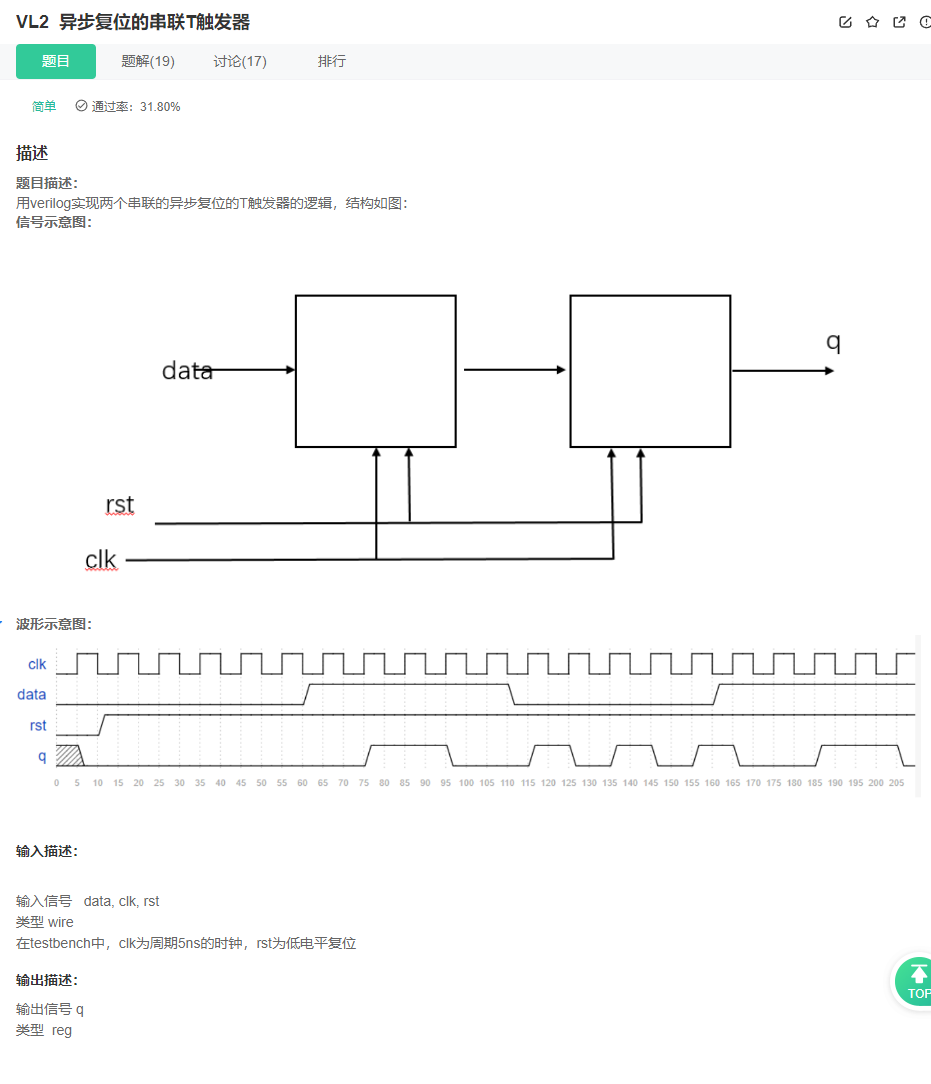
答案
`timescale 1ns/1ns
module Tff_2 (
input wire data, clk, rst,
output reg q
);
//*************code***********//
    reg tmp;
    always@(posedge clk or negedge rst)begin
        if (!rst)
            tmp <= 1'd0;
        else if (data)
            tmp <= ~tmp;
        else
            tmp <= tmp;
    end

    always@(posedge clk or negedge rst)begin
        if (!rst)
            q <= 1'd0;
        else if (tmp)
            q <= ~q;
        else
            q <= q;
    end
//*************code***********//
endmodule
分析
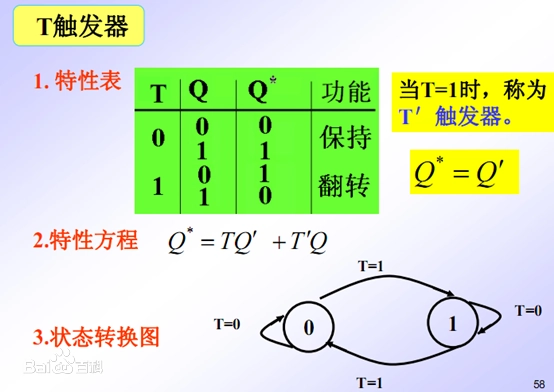
- 从上面这张图可以得出:T 触发器的核心要点,来 1 翻转,来 0 保持。
- 根据原理,就很容易得到上面的答案。但是,注意观察真值表,还会得到逻辑表达式:
Q* = T ^ Q,于是可以将核心代码简化:
//*************code***********//
    reg tmp;
    always@(posedge clk or negedge rst)begin
        if (!rst)
            tmp <= 1'd0;
        else
            tmp <= data ^ tmp;
    end

    always@(posedge clk or negedge rst)begin
        if (!rst)
            q <= 1'd0;
        else
            q <= tmp ^ q;
    end
//*************code***********//
- 注意思考,T 触发器的核心要点,来 1 翻转,来 0 保持。可以不可以理解为,门控时钟的一种体现?
复盘
注意 T 触发器:来 1 翻转,来 0 保持。
注意理解同步复位和异步复位。
异步复位的缺点:产生毛刺(容易造成亚稳态)
同步复位的缺点:同步复位的电路实现,比异步复位的电路实现,要浪费更多电路资源
关于浪费资源这一点,由于很多fpga自带异步复位,所以同步复位会多增加一个mux
那么结合两者,避免产生亚稳态的同时也充分利用资源,可以采用异步复位同步释放。
常用的异步复位同步释放图:
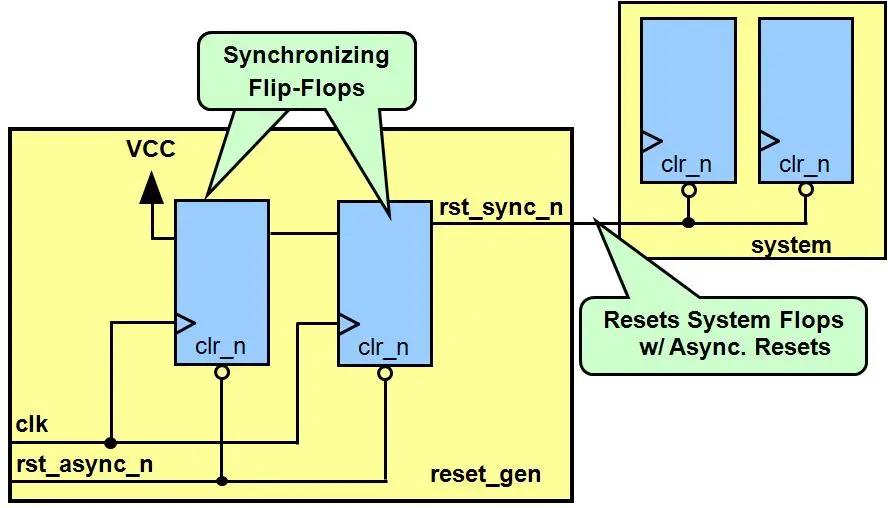
这里博客中给出了一系列经常容易迷惑的点的解答
1.直接接入异步复位信号驱动复位端有啥问题?
就是常说的异步复位产生亚稳态
2.两级触发器同步,就能消除亚稳态吗?
不能,但能大大减少
3.如果只做一级触发器同步,如何?
不可以。第一级触发器的输出,永远存在亚稳态的可能。亚稳态,导致系统不会复位初始化到已知状态。
当第一级触发器采样异步输入之后,允许输出出现的亚稳态可以长达一个周期,在这个周期内,亚稳态特性减弱。在第二个时钟沿到来时,第二级同步器采样,之后才把该信号传递到内部逻辑中去。第二级输出是稳定且已被同步了的。如果在第二级采样时保持时间不够,第一级的输出仍然处于很强的亚稳态,将会导致第二级同步器也进入亚稳态,但这种故障出现的概率比较小。
4.复位同步器,第2个dff是否存在亚稳态?(这个最让人迷惑)
只有当DFF的数据输入端口和数据输出端口,存在值不同的情况下,才会有recovery timing/removal timing问题。
第1个dff的数据输入端口和数据输出端口,在异步复位释放的时刻,是1和0,所以会有竞争冒险,有概率产生亚稳态;
第2个dff的数据输入端口和数据输出端口,在异步复位释放的时刻,是0和0,所以不存在竞争冒险,不会产生亚稳态。
因为第1个dff有概率产生亚稳态,为了防止传播,所以,多加几级dff,降低亚稳态的传播概率是有益处的。
上面九成问题的答案都转自博客,需要强调的是,现代数字芯片设计,强调的都是同步复位,这样有利于STA(静态时序分析),便于移植。
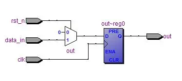
RTL原理图如下:
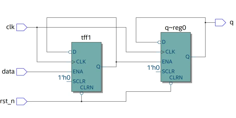
这里Q和D连接我认为可能是逻辑表达式要求和当前状态有关,但说实话,我不清楚这两个模块RTL内部的结构,无法做进一步分析。
测试代码如下:
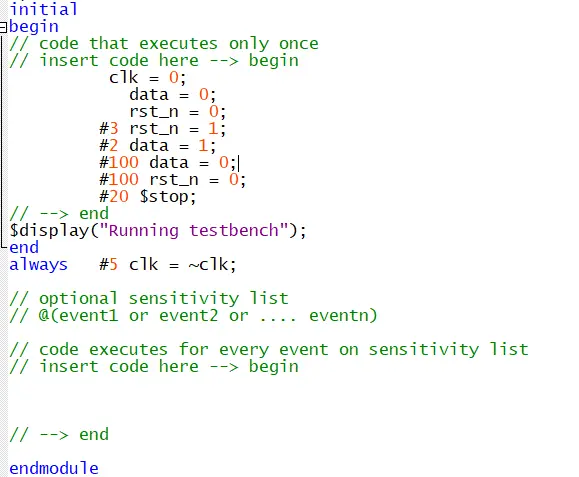
主要就是clk和data数据的编写
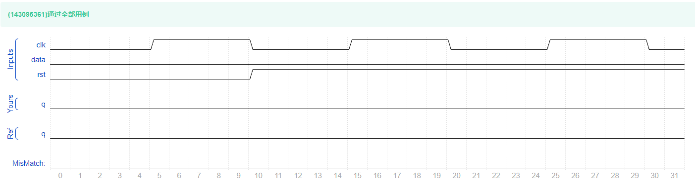
得到的仿真波形如下:

-
当data为1的时刻,时钟一旦采样到,下一个时钟上升沿则中间输出翻转,而中间输出每两个时钟周期产生一次持续一个周期的高电平,这带来最终输入翻转,每次翻转应该为两个周期一次。且滞后一个周期。
-
当data为0的时候,若中间输出为一,最终输出继续翻转,若为零,保持不变(波形仅仅涵盖第二种结果。
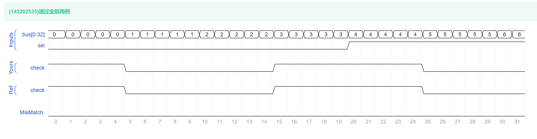
VL3 奇偶校验
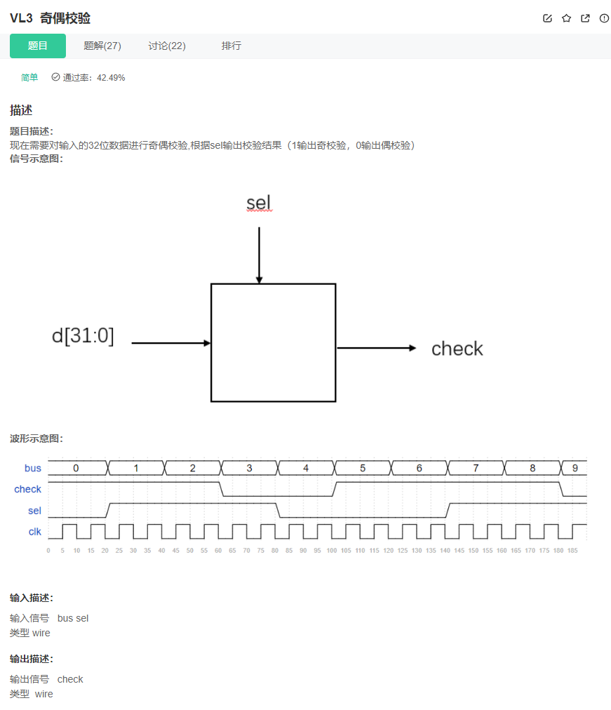
答案
`timescale 1ns/1ns
module odd_sel(
input [31:0] bus,
input sel,
output check
);
//*************code***********//

    assign check = sel ? (^bus) : ~(^bus);

//*************code***********//
endmodule
分析
1、奇偶校验,通过校验位使得1的个数恰好是奇数个或偶数个
奇校验:原始码流+校验位 总共有奇数个1
偶校验:原始码流+校验位 总共有偶数个1
说人话,
对于奇校验,如果原始码流中1的个数是偶数个,那么校验位就是1, 否则就是0;
对于奇校验,如果原始码流中1的个数是奇数个,那么校验位就是0, 否则就是1;
对于偶校验,如果原始码流中1的个数是偶数个,那么校验位就是0, 否则就是1;
对于偶校验,如果原始码流中1的个数是奇数个,那么校验位就是1, 否则就是0;
2、判断原始码流中的1的个数是偶数个还是奇数个
- 此处很容易想到异或操作,
0011_1111_1111_1111按位异或得到的值是1,此时的1就是奇校验位;如果求偶校验位,取反即可
3、写出伪代码如下:
if (sel == 1)//求奇校验
	check = ^bus;
else
	check = ~(^bus);
- 此时很容易想到三目运算符写答案:
assign check = sel ? (^bus) : ~(^bus);
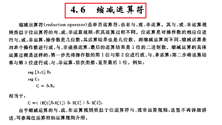
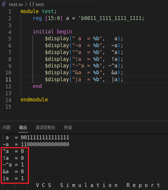
复盘
- 此处注意思考,
单目运算符和缩减运算符。需要对其一个概念,缩减运算符是单目运算符,但是单目运算符不一定是缩减运算符。
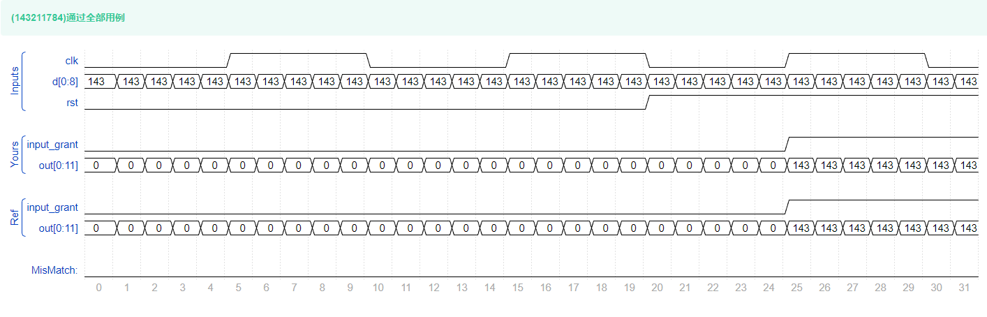
VL4 移位运算与乘法
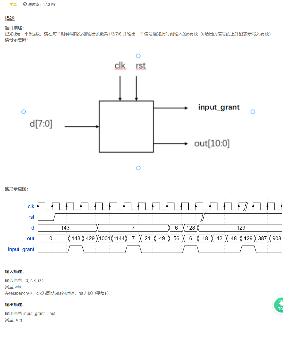
答案
`timescale 1ns/1ns
module multi_sel(
input [7:0]d ,
input clk,
input rst,
output reg input_grant,
output reg [10:0]out
);
//*************code***********//
    reg[1:0] cnt_4;
    always@(posedge clk or negedge rst)begin
        if(!rst)
            cnt_4 <= 'd0;
        else if(cnt_4 == 2'b11)
            cnt_4 <= 'd0;
        else cnt_4 <= cnt_4 + 1'b1;
    end

    reg [7:0] d_reg;
    always@(posedge clk or negedge rst)begin
        if(!rst)begin
                input_grant <= 'b0;
                out <= 'd0;
        end
        else if(cnt_4 == 'd0)begin
                input_grant <= 'b1;
                d_reg <= d;
                out <= d;
        end
        else if(cnt_4 == 'd1)begin
                input_grant <= 'b0;
                out <= d_reg * 3;
        end

         else if(cnt_4 == 'd2)begin
                input_grant <= 'b0;
                out <= d_reg * 7;
        end

            else if(cnt_4 == 'd3)begin
                input_grant <= 'b0;
                out <= d_reg * 8;
        end
    end
//*************code***********//
endmodule
复盘
- 题目中明确给出了四拍处理一个输入,很常见的就是设置一个计数器,用两位的计数器就可以统计四个状态,
也不用自己计数清零了。 - 上述的使用了带有优先级的
if -else结构,可以优化为case结构,小编就不改写这部分了,下一题用到了case结构。 - 上面的信号可以单独分开书写,优化效果如下:
//*************code***********//
    reg[1:0] cnt_4;
    always@(posedge clk or negedge rst)begin
        if(!rst)
            cnt_4 <= 'd0;
        else
            cnt_4 <= cnt_4 + 1'b1;
    end

    reg [7:0] d_reg;
    always@(posedge clk or negedge rst)begin
        if(!rst)begin
            input_grant <= 'b0;
            out <= 'd0;
        end
        else if(cnt_4 == 'd0)begin
            d_reg <= d;
            out <= d;
        end
        else if(cnt_4 == 'd1)begin
            out <= d_reg * 3;
        end
         else if(cnt_4 == 'd2)begin
            out <= d_reg * 7;
        end
        else if(cnt_4 == 'd3)begin
            out <= d_reg * 8;
        end
    end

    always@(posedge clk or negedge rst)begin
        if(!rst)begin
            input_grant <= 'b0;
        end
        else if(cnt_4 == 'd0)begin
            input_grant <= 'b1;
        end
        else begin
            input_grant <= 'b0;
        end
    end
//*************code***********//
VL5 位拆分与运算
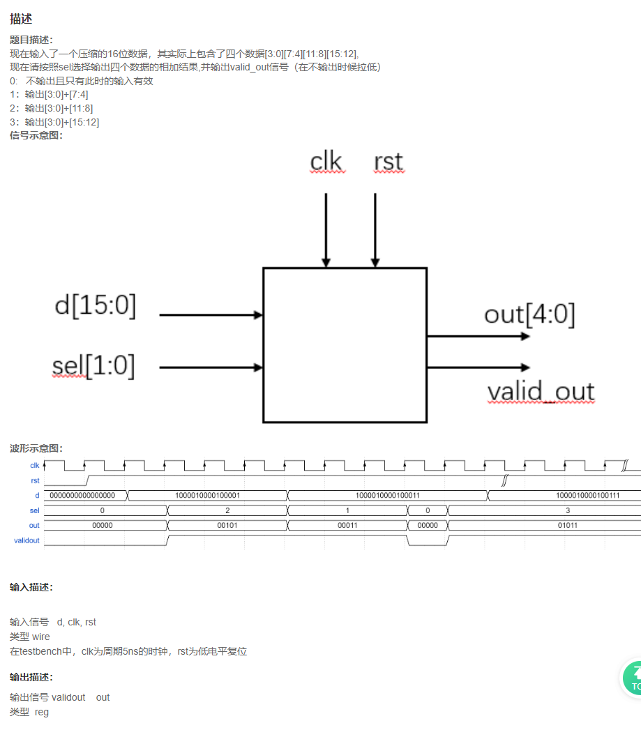
答案
`timescale 1ns/1ns

module data_cal(
input clk,
input rst,
input [15:0]d,
input [1:0]sel,

output [4:0]out,
output validout
);
//*************code***********//
    reg validout;
    always @ (posedge clk or negedge rst)begin
        if (!rst)begin
            validout <= 1'b0;
        end
        else if (sel == 2'b0) begin
            validout <= 1'b0;
        end  else begin
            validout <= 1'b1;
        end
    end

    reg [15:0] d_reg;
    always @ (posedge clk or negedge rst)begin
        if (!rst)begin
            d_reg <= 'd0;
        end
        else if (sel == 0)begin
            d_reg <= d;
        end
//         else begin
//             d_reg <= d_reg;
//         end
    end

    reg [4:0]out;
    always @ (posedge clk or negedge rst)begin
        if (!rst)begin
            out <= 'd0;
        end
        else case(sel)
            2'b00:out <= 'd0;
            2'b01:out <= d_reg[3:0] + d_reg[7:4];
            2'b10:out <= d_reg[3:0] + d_reg[11:8];
            2'b11:out <= d_reg[3:0] + d_reg[15:12];
        endcase
    end
//*************code***********//
endmodule
复盘
- 注意思考
d_reg的作用,这个信号究竟起着什么作用,还有注释掉的三行代码在工程实践中是否可以完全省略? case 结构怎么与if-else结构互换?
VL6 多功能数据处理器
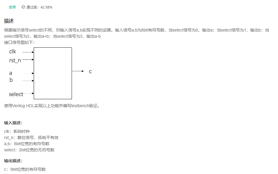
答案
`timescale 1ns/1ns
module data_select(
	input clk,
	input rst_n,
	input signed[7:0]a,
	input signed[7:0]b,
	input [1:0]select,
	output reg signed [8:0]c
);

    always@(posedge clk or negedge rst_n)begin
        if (!rst_n)
            c <= 'd0;
        else case(select)
            2'b00:c <= a;
            2'b01:c <= b;
            2'b10:c <= a+b;
            2'b11:c <= a-b;
        endcase
    end
endmodule
复盘
- 有没有觉得和上面几道题思路完全一致
VL7 求两个数的差值
答案
`timescale 1ns/1ns
module data_minus(
	input clk,
	input rst_n,
	input [7:0]a,
	input [7:0]b,

	output  reg [8:0]c
);
    always@(posedge clk or negedge rst_n)
    if (!rst_n)
            c <= 'd0;
    else
        c <= (a > b) ? (a - b) : (b-a);
endmodule
VL8 使用generate…for语句简化代码
答案
`timescale 1ns/1ns
module gen_for_module(
    input [7:0] data_in,
    output [7:0] data_out
);
    genvar i;
    generate for( i = 0; i < 8; i = i + 1 )
//         begin:generate_1
            assign data_out [i] = data_in [7 - i];
//         end
    endgenerate

endmodule
复盘
- 下面是别人写的笔记,请看小编上面的答案,还故意把第2条信息给违背了?
WHY?想必你可以自行判断正误
- 还有注意第一条为什么需要满足?个人觉得可以结合
动态变量进行理解!
VL9 使用子模块实现三输入数的大小比较
答案
`timescale 1ns/1ns
module main_mod(
	input clk,
	input rst_n,
	input [7:0]a,
	input [7:0]b,
	input [7:0]c,

	output [7:0]d
);

    wire [7:0] min1, min2;

   min_mod min1_mod(
       .clk(clk),
       .rst_n(rst_n),
       .a(a),
       .b(b),
       .min(min1)
   );

    min_mod min2_mod(
        .clk(clk),
        .rst_n(rst_n),
        .a(a),
        .b(c),
        .min(min2)
   );

    min_mod min3_mod(
        .clk(clk),
        .rst_n(rst_n),
        .a(min1),
        .b(min2),
        .min(d)
   );
//     assign d = min1 > min2 ? min2 : min1;
endmodule


module min_mod(
	input clk,
	input rst_n,
	input [7:0]a,
	input [7:0]b,

    output reg [7:0]min
);
    always@(posedge clk or negedge rst_n)
        if(!rst_n)
            min <= 'd0;
        else
            min <= (a > b) ? b : a;

endmodule
复盘
- 题目中要求使用子模块进行大小比较
- 注意时序要求:本想着节约一拍的时间,就写成了如下的形式,给报错了。
`timescale 1ns/1ns
module main_mod(
	input clk,
	input rst_n,
	input [7:0]a,
	input [7:0]b,
	input [7:0]c,

	output [7:0]d
);

    wire [7:0] min1, min2;

   min_mod min1_mod(
       .clk(clk),
       .rst_n(rst_n),
       .a(a),
       .b(b),
       .min(min1)
   );

    min_mod min2_mod(
        .clk(clk),
        .rst_n(rst_n),
        .a(a),
        .b(c),
        .min(min2)
   );

//     min_mod min3_mod(
//         .clk(clk),
//         .rst_n(rst_n),
//         .a(min1),
//         .b(min2),
//         .min(d)
//    );

    assign d = min1 > min2 ? min2 : min1;

endmodule


module min_mod(
	input clk,
	input rst_n,
	input [7:0]a,
	input [7:0]b,

    output reg [7:0]min
);
    always@(posedge clk or negedge rst_n)
        if(!rst_n)
            min <= 'd0;
        else
            min <= (a > b) ? b : a;

endmodule
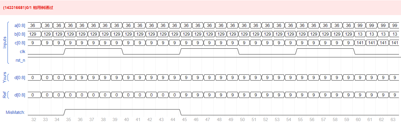
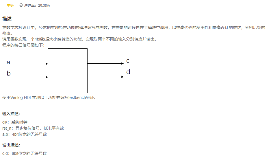
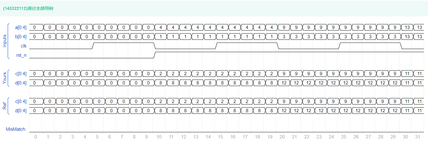
VL10 使用函数实现数据大小端转换
答案
`timescale 1ns/1ns
module function_mod(
    input clk,
    input rst_n,
	input [3:0]a,
	input [3:0]b,

	output [3:0]c,
	output [3:0]d
);

    function [3:0] reverse;
        input [3:0] data_in;
        begin
            reverse[0] = data_in[3];
            reverse[1] = data_in[2];
            reverse[2] = data_in[1];
            reverse[3] = data_in[0];
        end
    endfunction

    assign c = reverse(a);
    assign d = reverse(b);
endmodule
复盘
- 不想过多的解释,题目中原始端口竟然没有
clk和rst_n,而且题目中还说,c和d都是8bit的。。。 - 大小端,是针对字节序而言的。此题可以说是比特位反转,再说,这一功能用
流操作一行代码就可以搞定,设计人员赶快学学systemverilog。
02. 组合逻辑
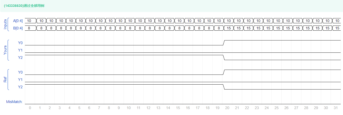
VL11 4位数值比较器电路
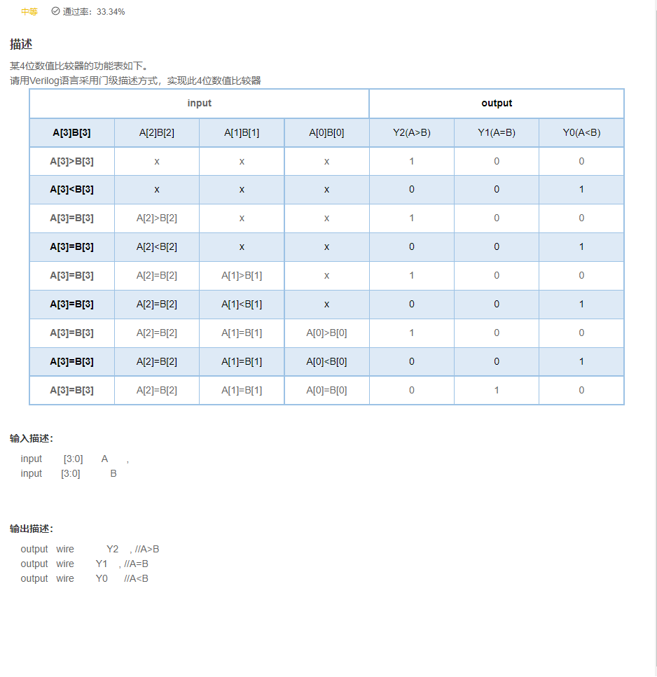
答案
`timescale 1ns/1ns

module comparator_4(
	input		[3:0]       A   	,
	input	   [3:0]		B   	,

 	output	 reg		Y2    , //A>B
	output   reg        Y1    , //A=B
    output   reg        Y0      //A<B
);

    always@(*)begin
        if (A[3] > B[3])
            {

    Y2,Y1,Y0} = 3'b100;
        else if (A[3] < B[3])
            {

    Y2,Y1,Y0} = 3'b001;
        else if (A[2] > B[2])
            {

    Y2,Y1,Y0} = 3'b100;
        else if (A[2] < B[2])
            {

    Y2,Y1,Y0} = 3'b001;

        else if (A[1] > B[1])
            {

    Y2,Y1,Y0} = 3'b100;
        else if (A[1] < B[1])
            {

    Y2,Y1,Y0} = 3'b001;
        else if (A[0] > B[0])
            {

    Y2,Y1,Y0} = 3'b100;
        else if (A[0] < B[0])
            {

    Y2,Y1,Y0} = 3'b001;
        else
            {

    Y2,Y1,Y0} = 3'b010;
    end

endmodule
复盘
- 上面全部使用了
if-else这种结构,它存在优先级关系,个人看来也是最容易理解的一种方式。 - 在实际项目中,并不是一下子就写出很稳健的程序,后期就是不断的优化,利用各种各样先进的算法、甚至加入设计模式来优化。
- 上面题目答案,我将接口定义的输出端口由
wire类型改为了reg类型,为什么呢?(自己想,就是不想打字了) - 接下面再将输出一致的情况合并,代码如下:
`timescale 1ns/1ns

module comparator_4(
	input		[3:0]       A   	,
	input	   [3:0]		B   	,

 	output	 reg		Y2    , //A>B
	output   reg        Y1    , //A=B
    output   reg        Y0      //A<B
);

    always@(*)begin
        if ((A[3] > B[3]) || ((A[3] == B[3]) &&  (A[2] > B[2])) || ((A[3] == B[3]) &&  (A[2] == B[2]) &&  (A[1] > B[1])) || ((A[3] == B[3]) &&  (A[2] == B[2]) &&  (A[1] == B[1]) &&  (A[0] > B[0])))
            {

    Y2,Y1,Y0} = 3'b100;
        else if ((A[3] < B[3]) || ((A[3] == B[3]) &&  (A[2] < B[2])) || ((A[3] == B[3]) &&  (A[2] == B[2]) &&  (A[1] < B[1])) || ((A[3] == B[3]) &&  (A[2] == B[2]) &&  (A[1] == B[1]) &&  (A[0] < B[0])))
            {

    Y2,Y1,Y0} = 3'b001;
        else
            {

    Y2,Y1,Y0} = 3'b010;
    end

endmodule
- 基于上述代码,继续优化,变量默认初始值都是0,我们只需要关注什么时候产生1,于是继续优化,代码如下:
`timescale 1ns/1ns

module comparator_4(
	input		[3:0]       A   	,
	input	   [3:0]		B   	,

 	output	 reg		Y2    , //A>B
	output   reg        Y1    , //A=B
    output   reg        Y0      //A<B
);

    always@(*)begin
            Y2 = ((A[3] > B[3]) || ((A[3] == B[3]) &&  (A[2] > B[2])) || ((A[3] == B[3]) &&  (A[2] == B[2]) &&  (A[1] > B[1])) || ((A[3] == B[3]) &&  (A[2] == B[2]) &&  (A[1] == B[1]) &&  (A[0] > B[0]))) ? 1'b1 : 1'b0;
            Y0 = ((A[3] < B[3]) || ((A[3] == B[3]) &&  (A[2] < B[2])) || ((A[3] == B[3]) &&  (A[2] == B[2]) &&  (A[1] < B[1])) || ((A[3] == B[3]) &&  (A[2] == B[2]) &&  (A[1] == B[1]) &&  (A[0] < B[0]))) ? 1'b1 : 1'b0;
            Y1 = ((A[3] == B[3]) &&  (A[2] == B[2]) &&  (A[1] == B[1]) &&  (A[0] == B[0]))  ? 1'b1 : 1'b0;
    end

endmodule
- 继续优化,Y1的逻辑可以简写成这样
Y1 = (A == B) ? 1'b1 : 1'b0;,甚至直接写成Y1 = A == B;还有三者的变量不同时为1,所以除Y1的变量可以写成其他两个变量取反
`timescale 1ns/1ns

module comparator_4(
	input		[3:0]       A   	,
	input	   [3:0]		B   	,

 	output	 reg		Y2    , //A>B
	output   reg        Y1    , //A=B
    output   reg        Y0      //A<B
);

    always@(*)begin
            Y2 = (A[3] > B[3]) || ((A[3] == B[3]) &&  (A[2] > B[2])) || ((A[3] == B[3]) &&  (A[2] == B[2]) &&  (A[1] > B[1])) || ((A[3] == B[3]) &&  (A[2] == B[2]) &&  (A[1] == B[1]) &&  (A[0] > B[0]));
            Y1 = A == B;
            Y0 = ~(Y2 || Y1);
    end

endmodule
- 此时此刻, 突然想把输出端口的reg类型改为原来的wire类型,那我们需要用assign语句了,继续改造,但是报错了,小编并不觉得错了,如果发现了错误可以在评论区指出来哈。
`timescale 1ns/1ns

module comparator_4(
	input		[3:0]       A   	,
	input	   [3:0]		B   	,

 	output	 wire		Y2    , //A>B
	output   wire       Y1    , //A=B
    output   wire       Y0      //A<B
);

    assign    Y1 = A == B;
    assign    Y2 = (A[3] > B[3]) || ((A[3] == B[3]) &&  (A[2] > B[2])) || ((A[3] == B[3]) &&  (A[2] == B[2]) &&  (A[1] > B[1])) || ((A[3] == B[3]) &&  (A[2] == B[2]) &&  (A[1] == B[1]) &&  (A[0] > B[0]));
    assign    Y0 = ~(Y2 || Y1);

endmodule
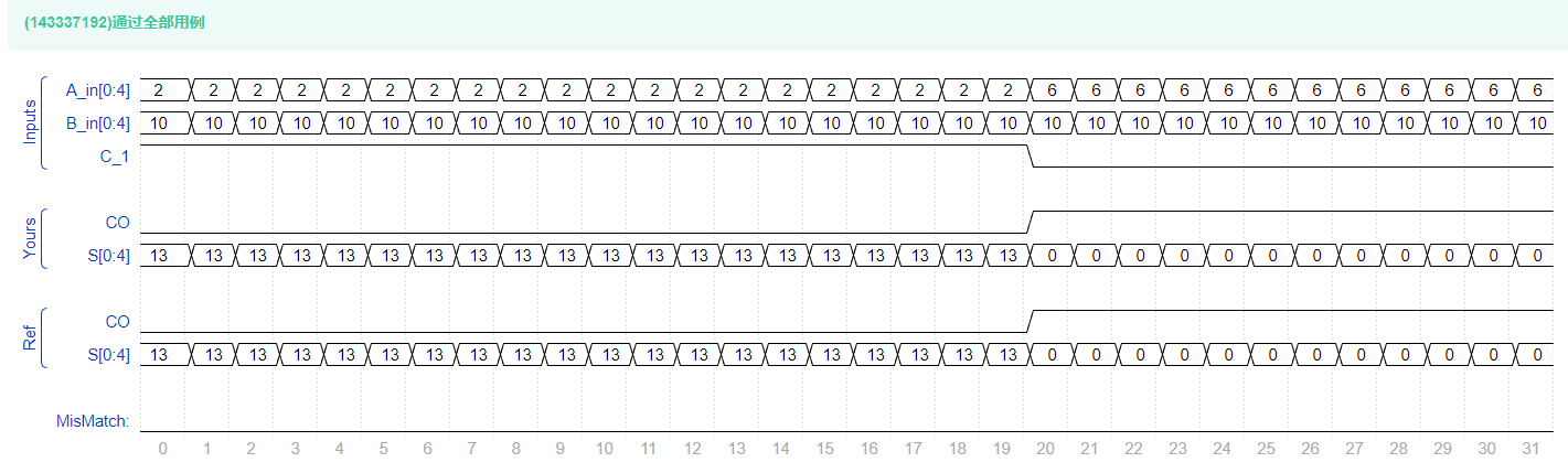
VL12 4bit超前进位加法器电路
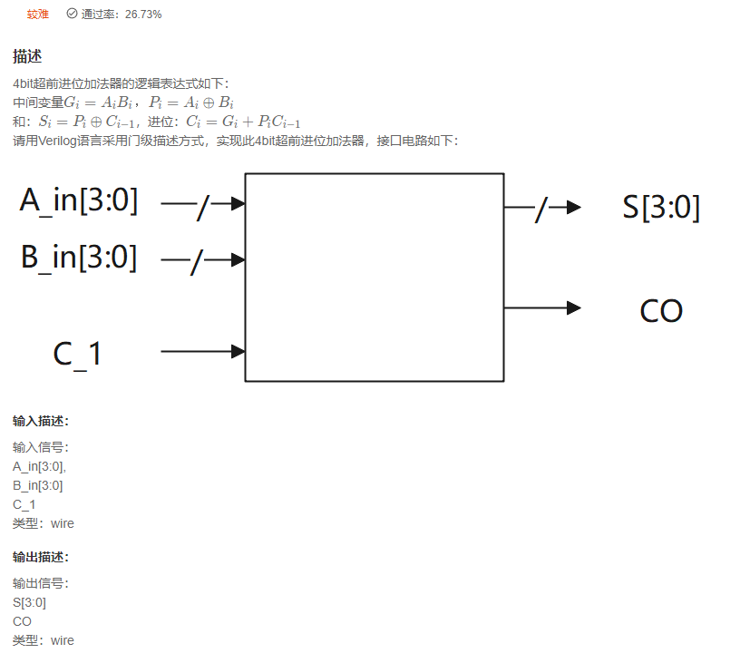
答案
`timescale 1ns/1ns

module lca_4(
	input		[3:0]       A_in  ,
	input	    [3:0]		B_in  ,
    input                   C_1   ,

 	output	 wire			CO    ,
	output   wire [3:0]	    S
);


    wire [3:0] G;
    wire [3:0] P;

    assign G[0] = A_in[0] & B_in[0];
    assign G[1] = A_in[1] & B_in[1];
    assign G[2] = A_in[2] & B_in[2];
    assign G[3] = A_in[3] & B_in[3];

    assign P[0] = A_in[0] ^ B_in[0];
    assign P[1] = A_in[1] ^ B_in[1];
    assign P[2] = A_in[2] ^ B_in[2];
    assign P[3] = A_in[3] ^ B_in[3];

    wire [3:0] C;

    assign S[0] = P[0] ^ C_1;
    assign S[1] = P[1] ^ C[0];
    assign S[2] = P[2] ^ C[1];
    assign S[3] = P[3] ^ C[2];
    assign CO = C[3];

    assign C[0] = G[0] | P[0]&C_1;
    assign C[1] = G[1] | P[1]&C[0];
    assign C[2] = G[2] | P[2]&C[1];
    assign C[3] = G[3] | P[3]&C[2];


endmodule
复盘
- 此处推荐一篇文章3-2 Verilog 4位行波进位加法器,还有可以了解一下
行波进位(Ripple Carry)与超前进位(Loodahead Carry) - 刚开始学习的时候就很迷糊,这部分就不展开胡说了。
VL13 优先编码器电路①
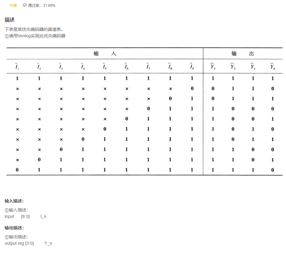
答案
`timescale 1ns/1ns

module encoder_0(
   input      [8:0]         I_n   ,

   output reg [3:0]         Y_n
);
    always @ (*)
      begin
        casex(I_n)
          9'b1_1111_1111 : Y_n = 4'b1111;
          9'b0_xxxx_xxxx : Y_n = 4'b0110;
          9'b1_0xxx_xxxx : Y_n = 4'b0111;
          9'b1_10xx_xxxx : Y_n = 4'b1000;
          9'b1_110x_xxxx : Y_n = 4'b1001;
          9'b1_1110_xxxx : Y_n = 4'b1010;
          9'b1_1111_0xxx : Y_n = 4'b1011;
          9'b1_1111_10xx : Y_n = 4'b1100;
          9'b1_1111_110x : Y_n = 4'b1101;
          9'b1_1111_1110 : Y_n = 4'b1110;
          default : Y_n = 4'b1111;
        endcase
      end
endmodule
复盘
- 答案已经在下一题给出了,哈哈哈
VL14 用优先编码器①实现键盘编码电路
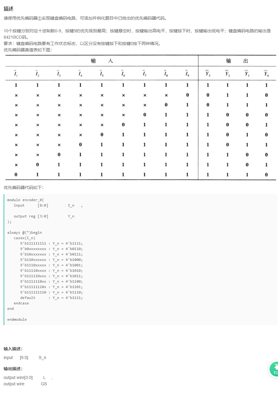
答案
`timescale 1ns/1ns
module encoder_0(
   input      [8:0]         I_n   ,

   output reg [3:0]         Y_n
);

always @(*)begin
   casex(I_n)
      9'b111111111 : Y_n = 4'b1111;
      9'b0xxxxxxxx : Y_n = 4'b0110;
      9'b10xxxxxxx : Y_n = 4'b0111;
      9'b110xxxxxx : Y_n = 4'b1000;
      9'b1110xxxxx : Y_n = 4'b1001;
      9'b11110xxxx : Y_n = 4'b1010;
      9'b111110xxx : Y_n = 4'b1011;
      9'b1111110xx : Y_n = 4'b1100;
      9'b11111110x : Y_n = 4'b1101;
      9'b111111110 : Y_n = 4'b1110;
      default      : Y_n = 4'b1111;
   endcase
end

endmodule

module key_encoder(
      input      [9:0]         S_n   ,

      output wire[3:0]         L     ,
      output wire              GS
);

    wire   [3:0]  Y_n;
    encoder_0 encoder(
       .I_n   (S_n[9:1]),
       .Y_n   (Y_n)
    );

    assign L = ~Y_n;
//     assign GS = ~(S_n[0] & Y_n[0] & Y_n[1] & Y_n[2] & Y_n[3]);
    assign GS = ((Y_n == 4'b1111) && (S_n[0] == 1)) ? 0 : 1;
endmodule
VL15 优先编码器Ⅰ
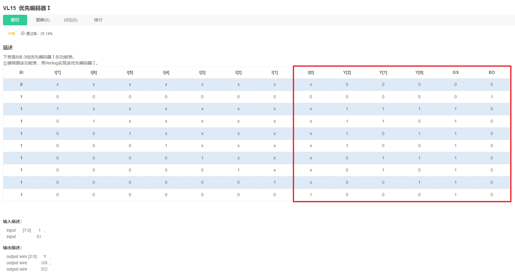
答案
`timescale 1ns/1ns

module encoder_83(
   input      [7:0]       I   ,
   input                  EI  ,

   output wire [2:0]      Y   ,
   output wire            GS  ,
   output wire            EO
);
    reg [4:0] temp;
    assign {

    Y[2:0],GS,EO} = temp;
    always@(*) begin
        casex({

    EI,I[7:0]})
            9'b0_xxxx_xxxx: temp =  5'b000_00;
            9'b1_0000_0000: temp =  5'b000_01;
            9'b1_1xxx_xxxx: temp =  5'b111_10;
            9'b1_01xx_xxxx: temp =  5'b110_10;
            9'b1_001x_xxxx: temp =  5'b101_10;
            9'b1_0001_xxxx: temp =  5'b100_10;
            9'b1_0000_1xxx: temp =  5'b011_10;
            9'b1_0000_01xx: temp =  5'b010_10;
            9'b1_0000_001x: temp =  5'b001_10;
            9'b1_0000_0001: temp =  5'b000_10;
        endcase
    end
endmodule
复盘
- 这种译码器最简单的实现方式就是,你把码表直接实现一遍即可。
- 比如,这部分的数字和题目中的完全一致
			9'b0_xxxx_xxxx: temp =  5'b000_00;
            9'b1_0000_0000: temp =  5'b000_01;
            9'b1_1xxx_xxxx: temp =  5'b111_10;
            9'b1_01xx_xxxx: temp =  5'b110_10;
            9'b1_001x_xxxx: temp =  5'b101_10;
            9'b1_0001_xxxx: temp =  5'b100_10;
            9'b1_0000_1xxx: temp =  5'b011_10;
            9'b1_0000_01xx: temp =  5'b010_10;
            9'b1_0000_001x: temp =  5'b001_10;
            9'b1_0000_0001: temp =  5'b000_10;
- 当然,还有其他实现方式,比如下题中给出的就是
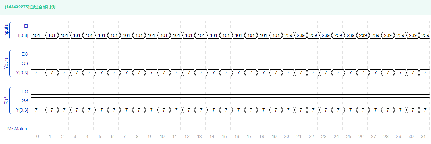
VL16 使用8线-3线优先编码器Ⅰ实现16线-4线优先编码器
答案
`timescale 1ns/1ns
module encoder_83(
   input      [7:0]       I   ,
   input                  EI  ,

   output wire [2:0]      Y   ,
   output wire            GS  ,
   output wire            EO
);
assign Y[2] = EI & (I[7] | I[6] | I[5] | I[4]);
assign Y[1] = EI & (I[7] | I[6] | ~I[5]&~I[4]&I[3] | ~I[5]&~I[4]&I[2]);
assign Y[0] = EI & (I[7] | ~I[6]&I[5] | ~I[6]&~I[4]&I[3] | ~I[6]&~I[4]&~I[2]&I[1]);

assign EO = EI&~I[7]&~I[6]&~I[5]&~I[4]&~I[3]&~I[2]&~I[1]&~I[0];

assign GS = EI&(I[7] | I[6] | I[5] | I[4] | I[3] | I[2] | I[1] | I[0]);
//assign GS = EI&(| I);

endmodule

module encoder_164(
   input      [15:0]      A   ,
   input                  EI  ,

   output wire [3:0]      L   ,
   output wire            GS  ,
   output wire            EO
);
    wire [2:0] Y_1,Y_0;
    wire gs_1,gs_0;
    wire EO1;

    encoder_83    encoder_83_U1(
        .I  (A[15:8]),
        .EI (EI),

        .Y  (Y_1),
        .GS (gs_1),
        .EO (EO1)
    );

    encoder_83    encoder_83_U0(
        .I (A[7:0]),
        .EI (EO1),

        .Y  (Y_0),
        .GS (gs_0),
        .EO (EO)
    );
    assign L = {

    gs_1,Y_1[2]|Y_0[2],Y_1[1]|Y_0[1],Y_1[0]|Y_0[0]};
    assign GS = gs_1|gs_0;

endmodule
复盘
- 抄的,题目晦涩难懂
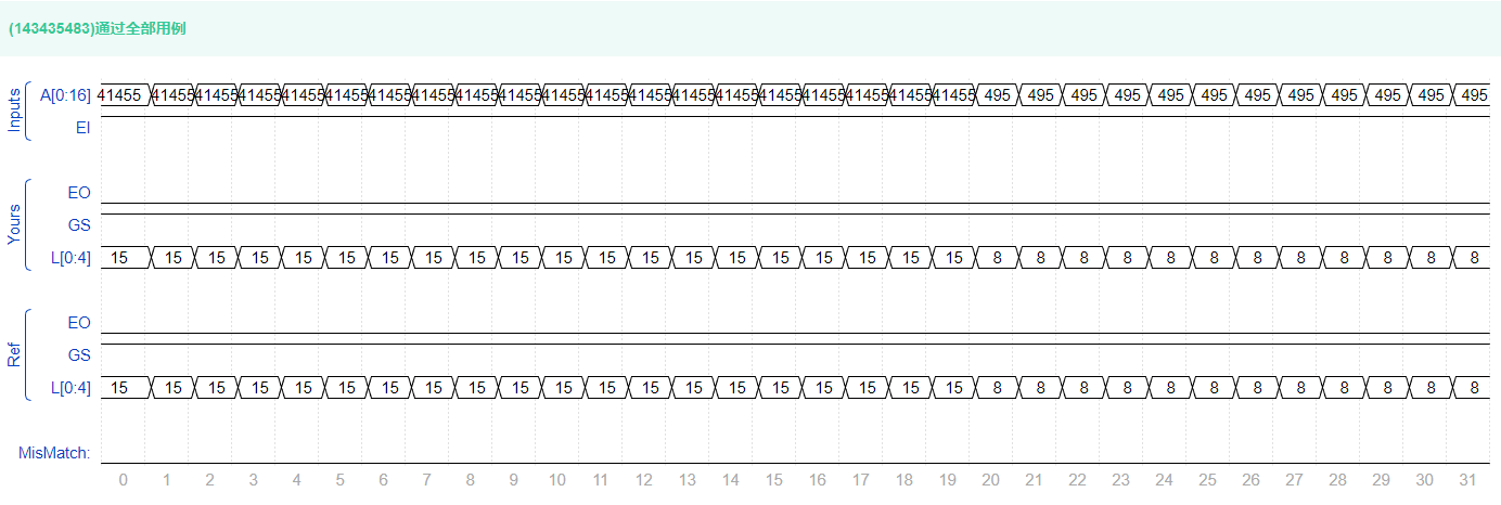
VL17 用3-8译码器实现全减器
答案
- 不想做,题目截图,防止后期题库更新就截图当快照了
VL18 实现3-8译码器①
中等 通过率:37.98%
描述
下表是74HC138译码器的功能表
①请用基础门电路实现该译码器电路,用Verilog将电路描述出来。基础门电路包括:非门、多输入与门、多输入或门。
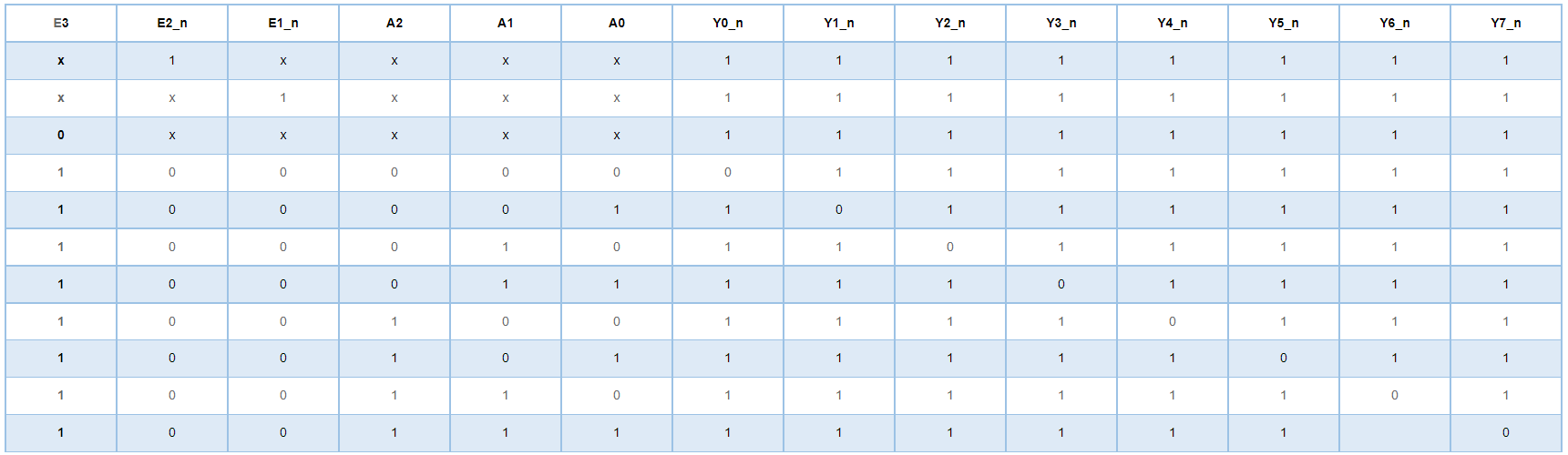
输入描述:
input E1_n ,
input E2_n ,
input E3 ,
input A0 ,
input A1 ,
input A2
输出描述:
output wire Y0_n ,
output wire Y1_n ,
output wire Y2_n ,
output wire Y3_n ,
output wire Y4_n ,
output wire Y5_n ,
output wire Y6_n ,
output wire Y7_n
答案
- 不想做,题目截图,防止后期题库更新就截图当快照了
VL19 使用3-8译码器①实现逻辑函数
- 略
VL20 数据选择器实现逻辑电路
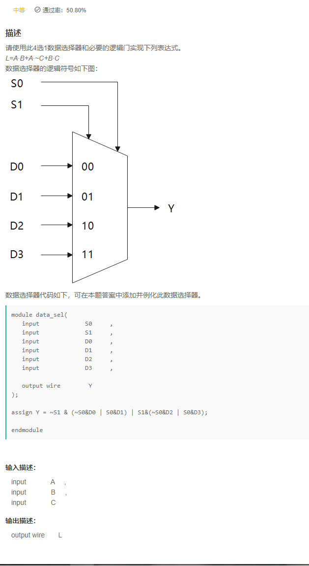
答案
`timescale 1ns/1ns

module data_sel(
   input             S0     ,
   input             S1     ,
   input             D0     ,
   input             D1     ,
   input             D2     ,
   input             D3     ,

   output wire        Y
);

assign Y = ~S1 & (~S0&D0 | S0&D1) | S1&(~S0&D2 | S0&D3);

endmodule

module sel_exp(
   input             A     ,
   input             B     ,
   input             C     ,

   output wire       L
);
    data_sel u(
        .S1('b0),
        .S0(C),

        .D1(B),
        .D0(A),
        .Y(L)
    );
endmodule
03. 时序逻辑
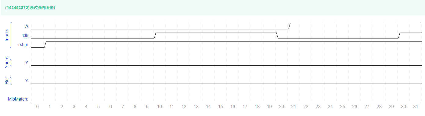
VL21 根据状态转移表实现时序电路
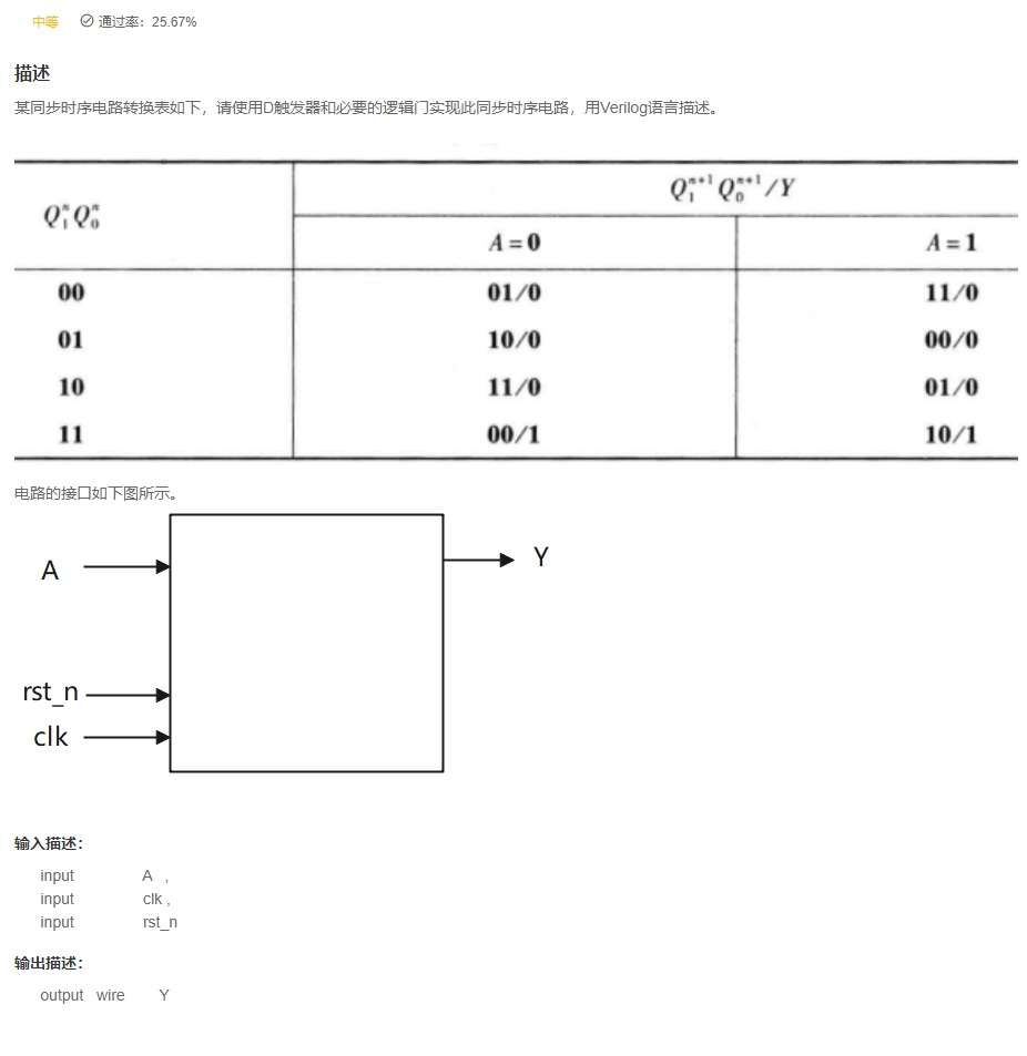
答案
`timescale 1ns/1ns

module seq_circuit(
      input                A   ,
      input                clk ,
      input                rst_n,

      output   wire        Y
);
    reg [1:0] cur_state,next_state;
    reg Y_temp;
    assign Y=Y_temp;

    parameter S0=2'b00;
    parameter S1=2'b01;
    parameter S2=2'b10;
    parameter S3=2'b11;

    always@(posedge clk or negedge rst_n)begin
        if(~rst_n)
            cur_state<=S0;
        else
            cur_state<=next_state;
    end

    always@(*)begin
        case(cur_state)
            S0:begin
                if(A==0)
                    next_state=S1;
                else
                    next_state=S3;
            end
            S1:begin
                if(A==0)
                    next_state=S2;
                else
                    next_state=S0;
            end
            S2:begin
                if(A==0)
                    next_state=S3;
                else
                    next_state=S1;
            end
            S3:begin
                if(A==0)
                    next_state=S0;
                else
                    next_state=S2;
            end
            default:next_state=S0;
        endcase
    end

    always@(*)begin
        if(cur_state==S3)
            Y_temp=1;
        else
            Y_temp=0;
    end

endmodule
复盘
-
下面这幅图能不能看懂
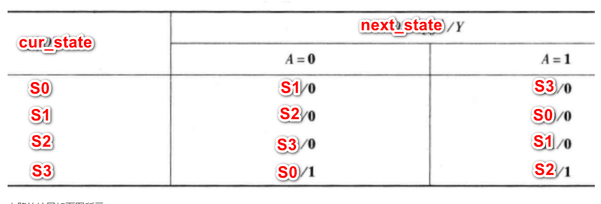
-
有了这个表再画出·状态转移图就相当于完成了
-
接下来尝试优化代码。
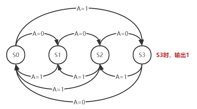
VL22 根据状态转移图实现时序电路
答案
`timescale 1ns/1ns

module seq_circuit(
   input                C   ,
   input                clk ,
   input                rst_n,

   output   wire        Y
);

    reg [1:0] cur_state,next_state;
    reg Y_temp;
    assign Y=Y_temp;

    parameter S0=2'b00;
    parameter S1=2'b01;
    parameter S2=2'b10;
    parameter S3=2'b11;

    always@(posedge clk or negedge rst_n)begin
        if(~rst_n)
            cur_state<=S0;
        else
            cur_state<=next_state;
    end

    always@(*)begin
        case(cur_state)
            S0:begin
                if(C==0)
                    next_state=S0;
                else
                    next_state=S1;
            end
            S1:begin
                if(C==0)
                    next_state=S3;
                else
                    next_state=S1;
            end
            S2:begin
                if(C==0)
                    next_state=S0;
                else
                    next_state=S2;
            end
            S3:begin
                if(C==0)
                    next_state=S3;
                else
                    next_state=S2;
            end
            default:next_state=S0;
        endcase
    end

    always@(*)begin
        if(cur_state==S3 || (cur_state==S2 && C == 1))
            Y_temp=1;
        else
            Y_temp=0;
    end


endmodule
复盘
- 直接修改上一题的代码就可以
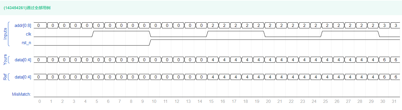
VL23 ROM的简单实现
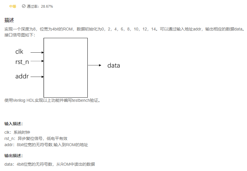
答案
`timescale 1ns/1ns
module rom(
	input clk,
	input rst_n,
	input [7:0]addr,

	output [3:0]data
);

    reg [3:0] romreg[7:0];

    always @ (posedge clk or negedge rst_n)
    begin
        if( ~rst_n ) begin
            romreg[0] <= 4'd0;
            romreg[1] <= 4'd2;
            romreg[2] <= 4'd4;
            romreg[3] <= 4'd6;
            romreg[4] <= 4'd8;
            romreg[5] <= 4'd10;
            romreg[6] <= 4'd12;
            romreg[7] <= 4'd14;
        end
//         else begin
//             romreg[0] <= 4'd0;
//             romreg[1] <= 4'd2;
//             romreg[2] <= 4'd4;
//             romreg[3] <= 4'd6;
//             romreg[4] <= 4'd8;
//             romreg[5] <= 4'd10;
//             romreg[6] <= 4'd12;
//             romreg[7] <= 4'd14;
//         end
    end

    assign data = romreg[addr];

endmodule
复盘
- 其实这个只读寄存器,初始化之后就不会改变了,因此只需要在
赋值的时候赋入初值即可,在实际项目中多通过读取Men配置文件来初始化。 - 有规律的初始化,肯定不会按个赋值了,找到规律,可以快速开发。优化代码如下:
`timescale 1ns/1ns
module rom(
	input clk,
	input rst_n,
	input [7:0]addr,

	output [3:0]data
);

    reg [3:0] romreg[7:0];
    integer i;
    always @ (posedge clk or negedge rst_n)
        if( ~rst_n ) begin
            for(i = 0; i < 8; i = i+1) begin : rom_i
                romreg[i] <= 2*i;
            end
        end

    assign data = romreg[addr];

endmodule
VL24 边沿检测
答案
`timescale 1ns/1ns
module edge_detect(
	input clk,
	input rst_n,
	input a,

	output reg rise,
	output reg down
);

    reg a_reg;

    always@(posedge clk or negedge rst_n)
        if(!rst_n)begin
            a_reg <= 1'b0;
            rise <= 1'b0;
            down <= 1'b0;
        end
        else begin
            a_reg <= a;
            if(a & ~a_reg)
                rise <= 1'b1;
            else
                rise <= 1'b0;
            if(~a & a_reg)
                down <= 1'b1;
            else
                down <= 1'b0;
        end

endmodule
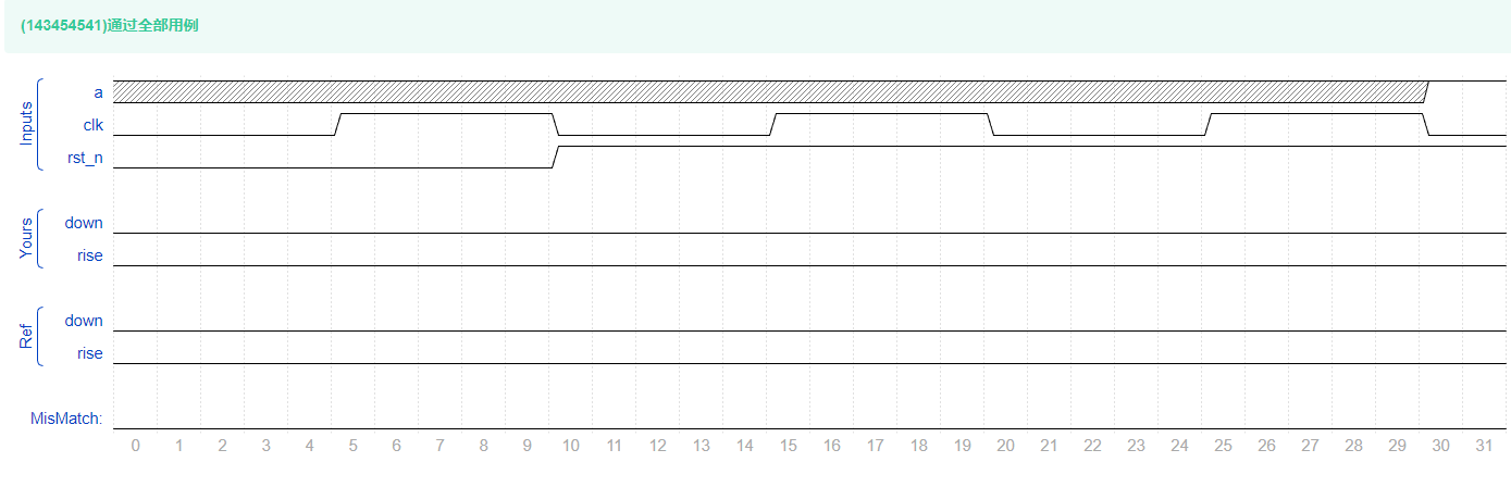
复盘
- 注意审题,题目中明确说到,
下一个时钟沿就拉高,意味着,不能再使用两级寄存器打两拍。
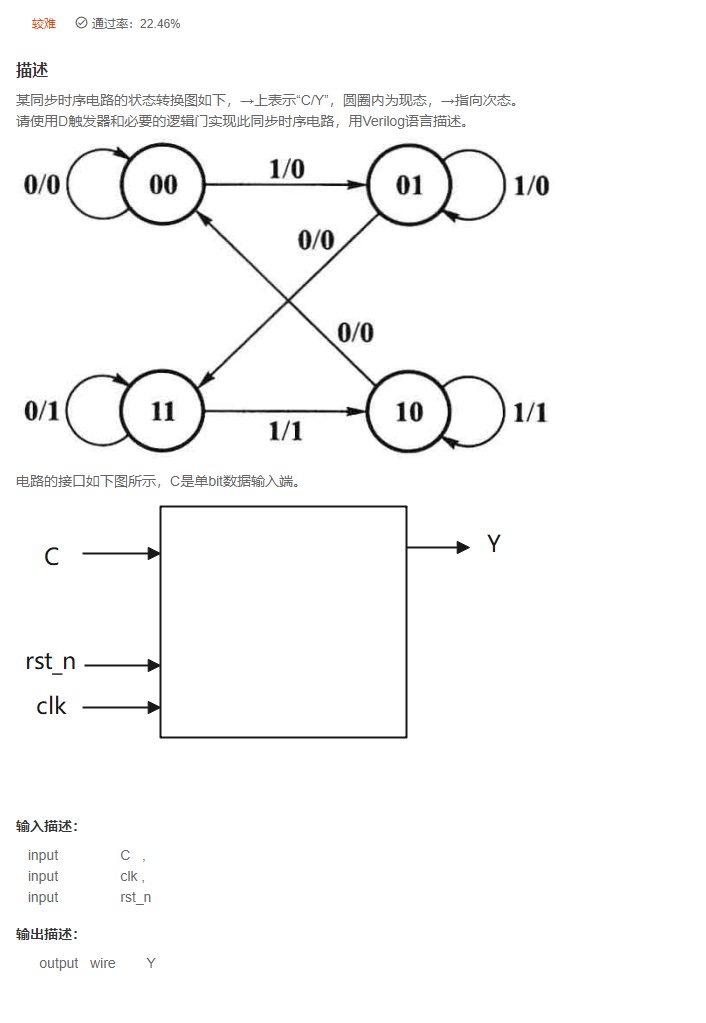
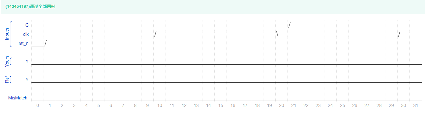
Part II Verilog进阶挑战
- 如果你想进阶学习,可以点击链接:《牛客刷verilog》Part II Verilog进阶挑战
Part III Verilog企业真题
- 如果你想练习真题,可以点击链接:《牛客刷verilog》Part III Verilog企业真题
后记
推荐相关文章