In order to reduce reflections during high-speed signal transmission, impedance matching must be maintained at the signal source, receiver, and transmission line. The exact impedance of a single-ended signal line depends on its width and its location relative to the reference plane. The line width/spacing between differential pairs required for a specific impedance depends on the chosen PCB stackup.
Since the minimum line width and minimum line spacing depend on the PCB type and cost requirements, the selected PCB stack structure must be able to meet all impedance requirements on the board, including inner and outer layers, single-ended and differential lines, etc. .
PCB stackup design
“
Layer Definition Design Principles
1. The adjacent layer of the main chip is the ground plane, which provides a reference plane for device surface wiring;
2. All signal layers should be adjacent to the ground plane as much as possible;
3. Try to avoid the two signal layers being directly adjacent;
4. The main power supply should be adjacent to its corresponding ground as much as possible;
5. In principle, a symmetrical structure design should be adopted. The meaning of symmetry includes: the thickness and type of the dielectric layer, the thickness of the copper foil, and the symmetry of the pattern distribution type (large copper foil layer, circuit layer).
“
PCB Layer Definition Recommendations
When setting specific PCB layers, it is necessary to flexibly grasp the above principles, determine the arrangement of layers according to actual needs, and avoid mechanically applying them. The common layer layout recommendations are given below for reference. When setting layers, if there are adjacent wiring layers, the interlayer crosstalk can be reduced by increasing the distance between adjacent wiring layers. For cross-segmentation, ensure that key signals must have a relatively complete reference ground plane or provide necessary bridging measures.
This article takes the PCB design of the RK3588 solution as an example. Its 10-layer 1st order, 10-layer 2nd order, and 8-layer through-hole PCB stack-up structures are introduced to help customers in the selection and evaluation of stacked structures. If you choose another type of stacked structure, please recalculate the impedance according to the specifications given by the PCB manufacturer.
This article uses the impedance calculation function of Huaqiu DFM software to explain the relevant stackup and impedance design cases. This is a domestic free PCB manufacturability and PCBA assembly analysis software that helps design engineers check out manufacturability problems before production, and can meet various usage scenarios that engineers need .
Huaqiu DFM software download address (copy to computer browser to open):
https://dfm.elecfans.com/uploads/software/promoter/hqdfm_DFMGZH.zip
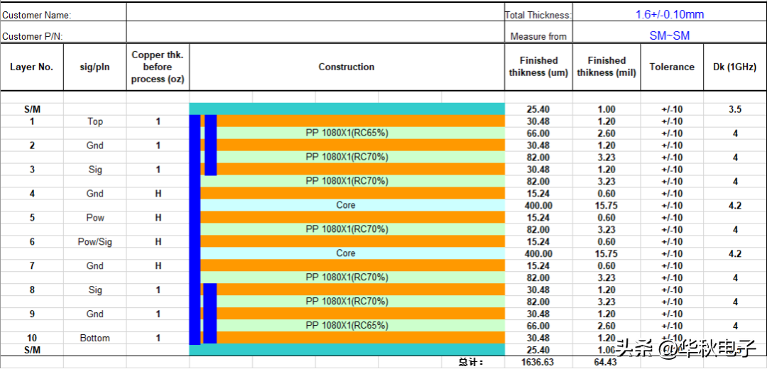
8-layer through-hole plate 1.6mm thickness stack design
In the 8-layer through-hole board stackup design, the reference plane of the top signal L1 is L2, and the reference plane of the bottom signal L8 is L7. The recommended stacking is TOP-Gnd-Signal-Power-Gnd-Signal-Gnd-Bottom. The thickness of the base copper is recommended to be 1oZ and the thickness is 1.6mm. The stacking design is shown in the figure below.

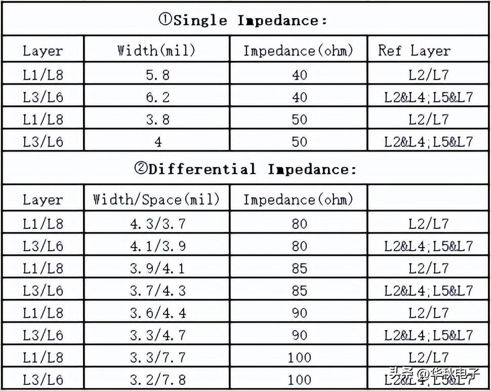
8-layer through-hole plate 1.6mm thickness impedance design
“
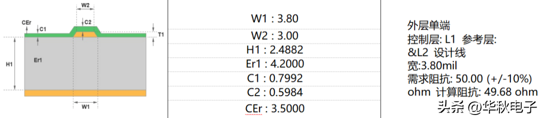
Outer single-ended 50 ohm impedance design
Using the Huaqiu DFM tool, select the single-ended impedance model of the outer layer, input the corresponding parameters, and calculate the corresponding line width to be 3.8mil, and the L1 and L8 layers are designed symmetrically, so the 50-ohm single-ended wiring of the L1 layer and the L8 layer is 3.8mil ,As shown below.
“
Outer layer differential 100 ohm impedance design
Using the Huaqiu DFM tool, select the single-ended impedance model of the outer layer, input the corresponding parameters, and calculate the corresponding line width/spacing to be 3.3/7.7mil, and the L1 and L8 layers are designed symmetrically, so the 100-ohm differential wiring between the L1 layer and the L8 layer It is 3.3/7.7mil, as shown in the figure below.

“
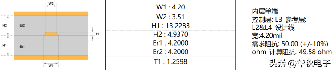
Inner single-ended 50 ohm impedance design
Use the Huaqiu DFM tool to select the single-ended impedance model of the outer layer, input the corresponding parameters, and calculate the corresponding line width to be 4.2mil, and the L3 and L6 layers are designed symmetrically, so the 50-ohm single-ended wiring of the L3 layer and the L6 layer is 4.2mil ,As shown below.
“
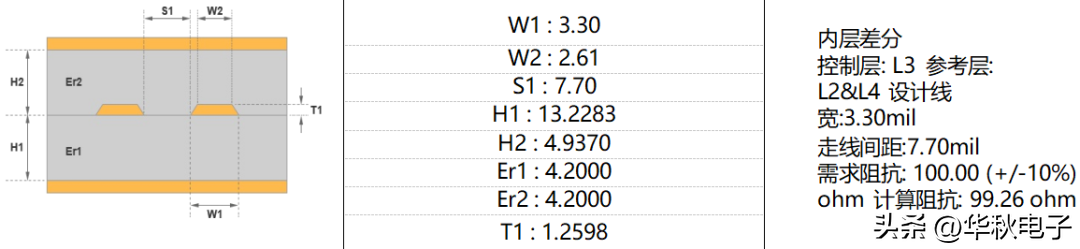
Inner differential 100 ohm impedance design
Use the Huaqiu DFM tool to select the single-ended impedance model of the outer layer, input the corresponding parameters, and calculate the corresponding line width/spacing as 3.3/7.7mil, and the L3 and L6 layers are designed symmetrically, so the 100-ohm differential wiring between the L3 layer and the L6 layer It is 3.3/7.7mil, as shown in the figure below.
“
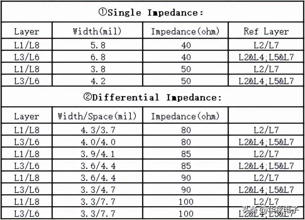
Overall Impedance Trace Width
8-layer through-hole plate 1.2mm thickness stack design
In the 8-layer through-hole board stackup design, the reference plane of the top signal L1 is L2, and the reference plane of the bottom signal L8 is L7. The recommended stacking is
TOP-Gnd-Signal-Power-Gnd-Signal-Gnd-Bottom. The thickness of the base copper is recommended to be 1oZ and the thickness is 1.2mm. The detailed stacking design is shown in the table below.

8-layer through-hole plate 1.2mm thickness impedance design
According to the stack design parameters, use Huaqiu DFM software to calculate the impedance. The calculation method is consistent with the above-mentioned 8-layer 1.6MM through-hole. The calculated impedance line width and line spacing are shown in the table below.
8-layer through-hole plate 1.0mm thickness stack design
In the 8-layer through-hole board stackup design, the reference plane of the top signal L1 is L2, and the reference plane of the bottom signal L8 is L7. The recommended stacking is
TOP-Gnd-Signal-Power-Gnd-Signal-Gnd-Bottom. The thickness of the base copper is recommended to be 1oZ and the thickness is 1.0mm. The detailed stacking design is shown in the table below.

1.0mm thickness impedance design for 8-layer through-hole board
According to the stack design parameters, use Huaqiu DFM software to calculate the impedance. The calculation method is consistent with the above-mentioned 8-layer 1.6MM through-hole. The calculated impedance line width and line spacing are shown in the table below.

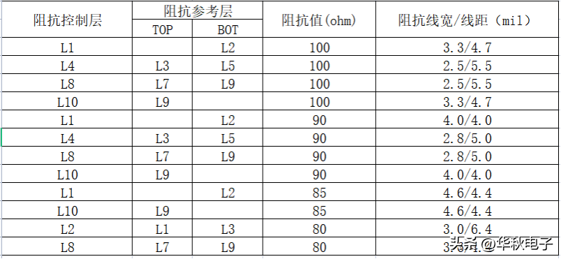
10-layer 1-stage HDI board with 1.6mm thickness stack-up design
In the 10-layer 1-stage board stack design, the reference plane of the top layer signal L1 is L2, and the reference plane of the bottom layer signal L10 is L9. It is recommended to stack as
TOP-Signal/Gnd-Gnd/Power-Signal-Gnd/Power-Gnd/Power-Gnd/Power-Signal-Gnd-Bottom, where L1, L2, L9, and L10 are recommended to use 1oZ, and other inner layers use HoZ. The figure below shows a reference stackup with a 1.6mm plate thickness.

Impedance design of 10-layer 1st-order HDI board with 1.6mm thickness
According to the stack design parameters, use Huaqiu dfm software to calculate the impedance. The calculation method is consistent with the above-mentioned 8-layer through-holes. Without taking screenshots one by one, the calculated single-ended impedance line width and line spacing and differential impedance line width and line spacing are shown in the figure below. Show.

10-layer 2-stage HDI board with 1.6mm thickness stack-up design
In the 10-layer 2-stage board stack design, the reference plane of the top signal L1 is L2, and the reference plane of the bottom signal L10 is L9. The recommended stacking is
TOP-Gnd-Signal-Gnd-Power-Signal/Pow-Gnd-Signal-Gnd-Bottom, where L1, L2, L3, L8, L9, and L10 are recommended to use 1oZ, and other inner layers use HoZ. The picture below shows a reference stackup with a 1.6mm board thickness.
10-layer 2-stage HDI board 1.6mm thickness impedance design
According to the stack design parameters, use Huaqiu dfm software to calculate the impedance. The calculation method is consistent with the above-mentioned 8-layer through-holes. Without taking screenshots one by one, the calculated single-ended impedance line width and line spacing and differential impedance line width and line spacing are shown in the figure below. Show.


Huaqiu DFM software download address (copy to computer browser to open):
https://dfm.elecfans.com/uploads/software/promoter/hqdfm_DFMGZH.zip