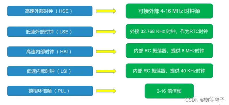
①HSI is a high-speed internal clock, RC oscillator with a frequency of 8MHz.
②HSE is a high-speed external clock, which can be connected to a quartz/ceramic resonator or an external clock source, and the frequency range is 4MHz~16MHz.
③ LSI is a low-speed internal clock, an RC oscillator with a frequency of 40kHz.
④LSE is a low-speed external clock connected to a quartz crystal with a frequency of 32.768kHz.
⑤PLL is the multiplier output of the phase-locked loop, and its clock input source can be selected as HSI/2, HSE or HSE/2. The frequency multiplier can be selected as 2~16 times, but the maximum output frequency should not exceed 72MHz.
1. Use an external crystal oscillator
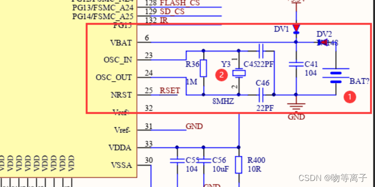
If an external crystal oscillator is used on the STM32, the connection of OSC_IN and OSC_OUT: an external high-speed crystal oscillator of 8MHz
2. Does not use an external crystal oscillator
If the internal RC oscillator is used instead of the external crystal oscillator, please proceed as follows:
① For 100-pin or 144-pin products, OSC_IN should be grounded, and OSC_OUT should be suspended.
② For products with less than 100 feet, there are 2 connection methods:
Type 1: OSC_IN and OSC_OUT are grounded through 10K resistors respectively. This method can improve EMC performance;
Type 2: Remap OSC_IN and OSC_OUT to PD0 and PD1 respectively, then configure PD0 and PD1 as push-pull output and output '0'. This approach reduces power consumption and saves (compared to above) 2 external resistors.
Starting from OSC_OUT and OSC_IN , these two pins are respectively connected to the external crystal oscillator 8MHz, the first frequency divider PLLXTPRE meets the switch PLLSRC (PLL entry clock source)
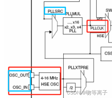
We can choose its output, the output is an external high-speed clock (HSE) or an internal high-speed clock (HSI). Here the output is selected as HSE

Then we encounter the phase-locked loop PLL, which has the function of frequency multiplication. Here we can input the frequency multiplication factor PLLMUL. If we want to overclock, we have to play tricks on this register. The clock passing through the PLL is called PLLCLK. We set the frequency multiplication factor to 9 multiplication, that is to say, after PLL, our clock changes from the original 8MHz HSE to 72MHz PLLCLK
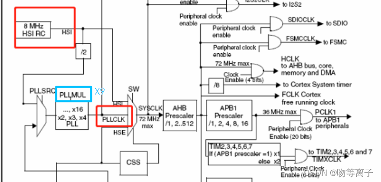
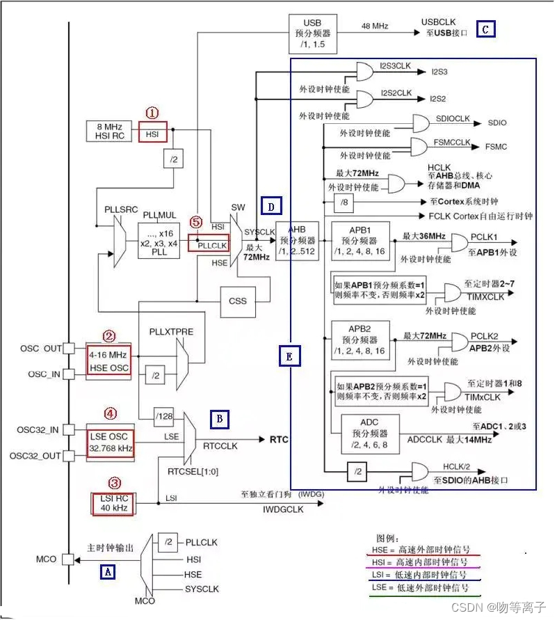
Immediately afterwards, a switch SW was encountered. After passing through this switch, it is the system clock (SYSCLK) of STM32. Through this switch, the clock source of SYSCLK can be switched, which can be selected as HSI, PLLCLK, and HSE.
We choose PLLCLK clock, so SYSCLK is 72MHz. Before PLLCLK is input to SW, it also flows to the USB prescaler, and the output of this divider is the clock (USBCLK) of the USB peripheral.

Returning to SYSCLK, SYSCLK passes through the AHB prescaler, and then is divided into other peripherals. Such as output to the clock called HCLK, FCLK, also directly output to the SDIOCLK clock of the SDIO peripheral, the FSMCCLK clock of the memory controller FSMC, and as the input of the prescaler of APB1 and APB2. GPIO peripherals are mounted on the APB2 bus
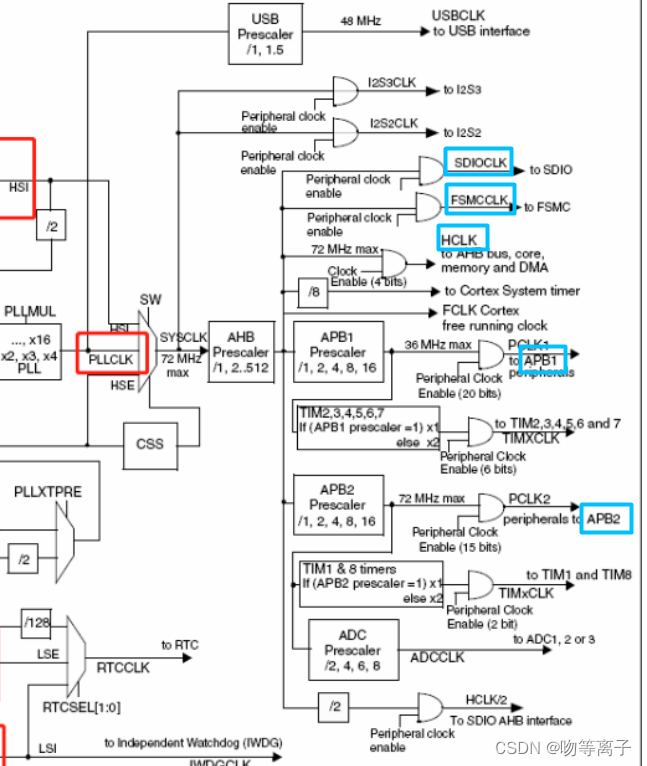
The clock of APB2 is the output of APB2 prescaler, and the clock source of APB2 prescaler is AHB prescaler. Therefore, if the APB2 prescaler is set to no frequency division, then we can get that the clock of the GPIO peripheral is also equal to HCLK, which is 72MHz.
SYSCLK: System clock, the clock source of most STM32 devices. Mainly distributed to various parts by the AHB prescaler.
HCLK: It is directly output by the AHB prescaler. It is the clock signal of the high-speed bus AHB, which is provided to the memory, DMA and cortex core. It is the clock for the operation of the cortex core. The main frequency of the cpu is this signal. Its size is the same as that of the STM32 operation Speed is closely related to data access speed.
FCLK: Also obtained from the output of the AHB prescaler, it is the "free running clock" of the core. "Free" means that it does not come from the clock HCLK, so FCLK also keeps running when the HCLK clock is stopped. Its existence can ensure that when the processor sleeps, it can also sample and interrupt and track sleep events, and it is synchronized with HCLK.
PCLK1: peripheral clock, obtained from the output of the APB1 prescaler, the maximum frequency is 36MHz, provided to the peripherals mounted on the APB1 bus, the peripherals on the APB1 bus are as follows:
RCC_APB1Periph_tiM2 TIM2 clock
RCC_APB1Periph_TIM3 TIM3 clock
RCC_APB1Periph_TIM4 TIM4 clock
RCC_APB1Periph_WWDG WWDG Clock
RCC_APB1Periph_SPI2 SPI2 clock
RCC_APB1Periph_USART2 USART2 Clock
RCC_APB1Periph_USART3 USART3 Clock
RCC_APB1Periph_I2C1 I2C1 Clock
RCC_APB1Periph_I2C2 I2C2 Clock
RCC_APB1Periph_USB USB Clock
RCC_APB1Periph_CAN CAN clock
RCC_APB1Periph_BKP BKP Clock
RCC_APB1Periph_PWR PWR clock
RCC_APB1Periph_ALL All APB1 peripheral clocks
PCLK2: peripheral clock, obtained from the output of the APB2 prescaler, the maximum frequency can be 72MHz, provided to the peripherals mounted on the APB2 bus, the peripherals on the APB2 bus are as follows:
RCC_APB2Periph_AFIO function multiplexing IO clock
RCC_APB2Periph_GPIOA GPIOA clock
RCC_APB2Periph_GPIOB GPIOB clock
RCC_APB2Periph_GPIOC GPIOC clock
RCC_APB2Periph_GPIOD GPIOD clock
RCC_APB2Periph_GPIOE GPIOE clock
RCC_APB2Periph_ADC1 ADC1 clock
RCC_APB2Periph_ADC2 ADC2 clock
RCC_APB2Periph_TIM1 TIM1 clock
RCC_APB2Periph_SPI1 SPI1 clock
RCC_APB2Periph_USART1 USART1 Clock
RCC_APB2Periph_ALL All APB2 peripheral clocks