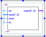
10)gg部分
library ieee;
use ieee.std_logic_1164.all;
entity gg is
port(we:in std_logic;
	input:in std_logic_vector(7 downto 0);
	clock:in std_logic;
	en:in std_logic;
	output:out std_logic_vector(7 downto 0):="11110110"
);
end gg;
architecture st of gg is
signal a:std_logic_vector(7 downto 0):="11110110";
begin
process(we,input)
begin
if (clock='0' and we='1') then
	a<=input;
elsif (clock='1' and en='1') then
	a<=input;
elsif (clock='1' and we='1') then
	a<=input;
end if;
end process;
output<=a;
end st;
接口设计:
Clock:时钟信号
we:使能信号
input:输入信号
output:输出信号
功能实现:
存储RAM输出的值,用于跳转JMP,JZ,JC三条指令的取跳转目的地址的操作。主要是用来稳定RAM的值,为了防止LPM_RAM_IO芯片可能会出现突变或者无输出等异常情况,所以采用这个来对指令信号进行稳定,并进行暂存,来帮助IR信号的稳定。而在JMP,JZ,JC这三条跳转指令里面,gg寄存器则起到了暂存目的地址,并将目的地址传递给PC的作用。
仿真验证:
与cpu在同一文件中,与cpu同仿真。
下篇点此
