For the novice, the first step to understand basic concepts of PCIE, PCIE second step to understand the configuration space, the third step in-depth study PCIE device enumeration method. This chapter summarizes the second step of the PCIE configuration space
According to international practice, to ask questions:
1. What is the configuration space of the PCIE?
2. PCIE device configuration space is how much? What is the difference between PCI and PCIE link configuration space?
3. How to access the configuration space PCIE devices?
4. There are several types, contains what?
With the above-described problems, the portion to be summarized:
What is the configuration space of the PCIE?
PCIE each device has its own separate section of the configuration space, the space is part of this device (possibly some e2prom), the system will allocate a section of memory the device space, CPU access this memory space that is, access to this device configuration space. Equipment at the factory, the configuration space is the default initial value.
PCIE device configuration space is how much? PCIE and PCI configuration space Contact What's the difference?
PCI early period, the system is only 256 Bytes memory size allocated to each PCI device. PCIE to the later period, with equipment performance enhancements, device configuration space PCIE expansion to a 4K Bytes. It should be noted here:
PCIE supports a total of 256 Bus, 32 Ge Dev, 8 Ge Fun. Therefore, in the case of full load, require a total memory size = 4k * 256 * 32 * 8 = 256K Bytes = 256M 256M memory space is the space system for the preparation of the PCIE device is not available, this is your memory, to the actual you will always be less than with one of the main nominal.
PCIE forward compatible PCI device, the first 256 Byte configuration space for each device is PCI access space, space after 4k-256 Byte for a PCIE expansion. This is the main difference between the two, a further distinction will lead the following questions
Access method PCI / PCIE device configuration space ---- IO access memory access
X86 system, the address mapping PCIE device configuration space there are two ways: IO memory mapping and mapping. So developers can also be accessed via IO or memory access to access its configuration space
PCIE access device inseparable from its Bus, Dev, Fun numbering, as shown in FIG register, Bit [23:16] is used to store Bus number, total 8Bit, thus explaining why the above expression, a total of 256 Bus, Bit [15:11] is stored Dev, you can store a total of 32 5bit Dev, Bit [10: 8] is stored Bus, can store a total of eight 3Bit Fun.
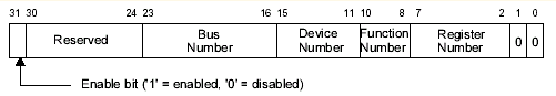
Whether using IO memory or way to access the configuration space, they are inseparable from the figure above, the following specific description:
1. IO access
IO should be a unique product of the Intel X86 architecture, it is understood as simply a period of storage, accessed by the user IN / OUT instructions (memory, then need to be accessed with the MOVE command), the device portion may be mapped to the IO space, developers port to access the device via IO, such as now presented this: CF8 / CFC. Intel can be accessed for the first 256 Byte PCIE through this set of ports, a specified address, a specified data. code show as below:
. 1  / * Writer DATE to CF8 * /
2 the Address BIT31 = | ((BUS & 0XFF ) << 16 ) | ((the DEV & 0x1F ) << . 11 ) | ((Fun & 0x7 ) << . 8 );
. 3 IoWrite32 ( 0xCF8 , address); // read address to be written to CF8
. 4 Date32 = IoRead32 ( 0xcfc ); // address of the port to read data from the CFC
Note: IO access can only read the first 256 Byte, space after 256Byte need access memory
2. Memory Access
This fact, and IO access similar, all configuration space mapped into memory, after determining that the user device address, can be accessed through the read-write memory, the following code:
1 /*Write date*/
2 MmioWrite32(PcieBaseAdd + Bus<<16 + Dev<<11 + Fun<<8 + offset, date); //PcieBaseAdd为PCIE在内存中的基地址
3
4 /*Read date*/
5 Value = MmioRead32(PcieBaseAdd + Bus<<16 + Dev<<11 + Fun<<8 + offset);
PCIE centralized configuration space type, contains what
There are two main configuration space, the developer can also clear these two, one Type0: space equipment Second Type1: Bridge space
As shown in FIG device space: The following describes the content, and wherein the major role:
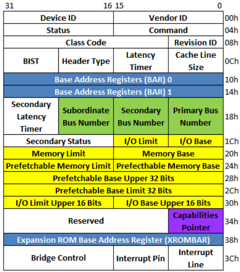
DID & VID: vendor ID and equipment, and each playing device should not be fixed, this is usually determined by the device ID enumeration apparatus determines whether or not there.
Class Code:
HeaderType:
BAR0 & BAR1: base address of the equipment space
Subordinate Bus Number: Number Bus Slave Bus Fengyun tree i.e. the maximum number of Bus.
Secondary Bus Number: Bus number connected at the Bridge
Primary Bus Number: pick on the Bridge Bus Number
Memory Limit: This device allocated memory size?
Memroy Base: This equipment, including base from which to allocate an address?