1. 配置IP核可以参考网上教程,有很多,这里不做赘述。注意的是本次使用的是单端口RAM, 在设置时,人为勾选了ena片选信号。
2. 关于配置RAM时的数据宽度和深度问题。
答: 数据宽度规定为8位, 数据深度本来定义18根地址总线[17:0],把深度在设置中定义为18。但在初始化端口中显示addr只有4位,故重新定义深度为2的18次方为262144。
3. 实例化RAM代码(verilog), 这里top文件包含4个IP核RAM,共用clk, wr_en, data_in,addr接口,ena片选信号有4位。 并且做了例化,例化时注意端口配置,例化名称两个问题。

 1 `timescale 1ns / 1ps
 2 //////////////////////////////////////////////////////////////////////////////////
 3 // Company:
 4 // Engineer:
 5 //
 6 // Create Date:    14:13:45 08/22/2018
 7 // Design Name:
 8 // Module Name:    test_bram
 9 // Project Name:
10 // Target Devices:
11 // Tool versions:
12 // Description:
13 //
14 // Dependencies:
15 //
16 // Revision:
17 // Revision 0.01 - File Created
18 // Additional Comments:
19 //
20 //////////////////////////////////////////////////////////////////////////////////
21 module test_bram
22 (
23     data_in, addr, ena, wr_en, clk, data_out1, data_out2, data_out3, data_out4
24 );
25
26 input wr_en, clk;
27 input [3:0] ena;
28 input [7:0] data_in;
29 output [7:0] data_out1;
30 output [7:0] data_out2;
31 output [7:0] data_out3;
32 output [7:0] data_out4;
33 input [17:0] addr;
34
35 wire wr_en, clk;
36 wire [3:0] ena;
37 wire [7:0] data_in;
38 wire [17:0] addr;
39 wire [7:0] data_out1;
40
41
42 inst_ram_1 inst1  //其中inst_ram是调用的子模块名称, inst1是在顶层模块中使用的实例名称。
43 (
44     .dina(data_in),
45     .clka(clk),
46     .ena(ena[0]),
47     .addra(addr),
48     .douta(data_out1),
49     .wea(wr_en)
50 );
51
52 inst_ram_1 inst2
53 (
54     .dina(data_in),
55     .clka(clk),
56     .ena(ena[1]),
57     .addra(addr),
58     .douta(data_out2),
59     .wea(wr_en)
60 );
61
62 inst_ram_1 inst3
63 (
64     .dina(data_in),
65     .clka(clk),
66     .ena(ena[2]),
67     .addra(addr),
68     .douta(data_out3),
69     .wea(wr_en)
70 );
71
72 inst_ram_1 inst4
73 (
74     .dina(data_in),
75     .clka(clk),
76     .ena(ena[3]),
77     .addra(addr),
78     .douta(data_out4),
79     .wea(wr_en)
80 );
81 endmodule
4. 各个模式的时序图
4.1 Write First Mode: In WRITE_FIRST mode, the input data is simultaneously written into memory and driven on the data output, as shown in Figure 9. This transparent mode offers the flexibility of using the data output bus during a write operation on the same port. (输入数据同时写入memory与data_output)
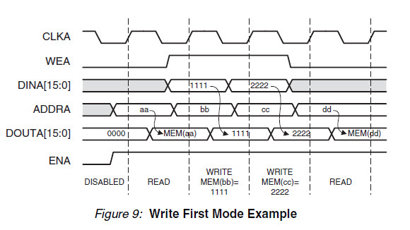
如上图所示,WEA为低电平,ENA 为低电平时,处于DISABLED状态。 在第一个READ状态中,WEA为低电平,ENA为高电平,故DOUTA输出为ADDR(aa)的数据。在WRITE MEM(bb)状态中,WEA为高电平,ENA为高电平,DIN为1111,输入到MEM与DOUTA中。 同理, WRITE MEM(cc)状态中,DOUTA为2222。最后一个READ状态,WEA为低电平,为读数据状态,故读出MEM(dd)的数据。
4.2 Read First Mode: In READ_FIRST mode, data previously stored at the write address appears on the data output, while the input data is being stored in memory. This read-before-write behavior is illustrated in figure 10. (先前存储在写地址处的数据出现在数据输出上,而输入数据存储在存储器中)
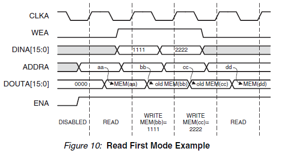
如上图所示,在WEA为高电平,且ENA为高电平时,DINA均写入到bb与cc的MEM中,而DOUTA输出先前存储在地址线的数据。
4.3 No Change Mode: In NO_CHANGE mode, the output latches remain unchanged during a write operation. As shown in Figure 11, the data output is still the previous read data and is unaffected by a write operation on the same port.(在写操作中,输出latched保持不变,output始终保持先前的值不受影响)

如上图所示,由No Change Mode的特性可知,虽然在WEA与ENA同时为高电平的时候,DOUTA依然为MEM(aa)的值。而DOUTA保持在WEA变换为低电平后,读取ADDR(dd)的值输出。
