RAM IP核
RAM: Random Access Memory, 随机存取存储器。
可以随时把数据写入任一指定地址的存储单元,也可以随时从任一指定地址中读出数据,将地址作为索引
读写速度是由时钟频率决定的。
作用: 主要用来存放程序以及程序执行过程中产生的中间数据、结果等
RAM IP核简介
通过对BRAM( 块RAM )存储器模块进行配置,可以实现各种存储器功能( RAM, 移位寄存器,ROM以及FIFO缓冲器 )
Block RAM资源, 一片是36K
每一片RAM有完全独立的读写端口
每一个端口都可以配置为32Kx1, 16Kx2, 8Kx4, 4Kx9(or8), 1Kx36(or 32), 512x72(or 64), 常用位宽为8,16,32
36K 资源不一定能够完全使用, 只有在特定的位宽才可以使用36K
每一块Block RAM可以被分割成独立的两块18K块RAM使用
所有的Block RAM的读写位宽都可以改变
两个邻近的36KBlock RAM,可以被配置成为一个64Kx1的双端口RAM
Vivado的BMG IP核( Block Memory Generator , 块RAM生成器),可以配置成RAM或者ROM。
- RAM,随机存取存储器,可读可写
- ROM, 只读存储器,正常工作时只读
两者使用资源都是FPGA内部的BRAM, 不过ROM只用到了BRAM的读数据端口。
RAM分类: 真双端口RAM, 伪双端口RAM,单端口RAM
- 真双端口RAM( True Dual-Port RAM, TDP), 两个端口都可以独立的对BRAM进行读写
- 伪双端口RAM( Simple Dual-Port RAM, SDP), 有两个端口,其中一个只能读,另一个只能写
- 单端口RAM, 只有一个RAM, 读写通过这一个端口来进行
单端口RAM只有一组数据线、地址线、时钟信号以及控制信号,双端口RAM具有两组数据线、地址线、时钟信号以及控制信号。
Xilinx 7系列的内部BRAM全部是真双端口RAM,两个端口可以独立的进行读写,可以被配置成不同的RAM形式。
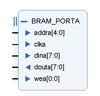
端口描述
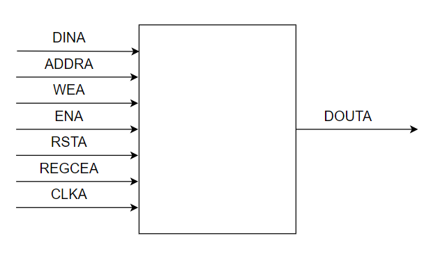
- DINA: 端口A写数据信号
- ADDRA: 端口A,读写地址信号,对于单端口RAM来说,读地址和写地址共用该地址线
- WEA: 端口A写使能信号,1->写有效,0->读有效
- ENA: 端口A写使能信号,高有效。禁止后端口A上的读写无效。ENA信号可选,取消该信号后,RAM一直处于有效状态。
- RSTA:端口A复位信号,可配置为高有效或者低有效,可选信号
- REGCEA: 端口A输出寄存器使能信号,为1时,DOUTA保持最后一次输出的数据,可选信号
- CLKA: 端口A的时钟信号
- DOUTA: 端口A读出的数据。
RAM IP核配置
-
Basic
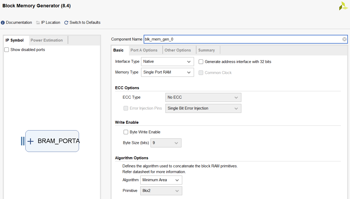
- Memory Type 存储器类型
- Single Port RAM (单端口RAM )
- Simple Dual Port RAM ( 伪双端口RAM )
- True Dual Port RAM ( 真双端口RAM )
- Single Port ROM ( 单端口ROM )
- Dual Port ROM ( 双端口ROM )
- ECC Options : Error Correction Capability 纠错能力选项 ( 单端口RAM不支持ECC )
- Write Enable: 字节写使能选项,勾选后可以单独将数据的某个字节写入RAM中
- Algorithm Options: 算法选项
- Minimum Area 最小面积
- Low Power 低功耗
- Fixed Primitives 固定原语
- Memory Type 存储器类型
-
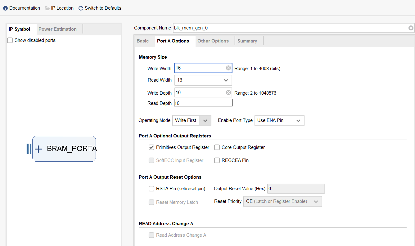
Port A 选项,设置端口A的参数
-
Write Width 写数据位宽( Bit )
-
Read Width
-
Write Depth 写深度,例如设置为32,RAM所能访问的地址范围为0-31
-
Read Depth
-
Operating Mode: RAM 读写操作模式,共三种模式
- Write First 写优先, 数据先写入RAM,然后在下一个时钟输出该数据
- Read First 读优先, 数据先写入RAM中,同时输出RAM中同地址的上一次数据
- No Change 不变模式,读写分开操作,不能同时进行
-
Enable Port Type: 使能端口类型
- Use ENA Pin 添加使能端口A信号
- Always Enabled 取消使能信号,端口一直处于使能状态
-
Port A Optional Output Register : 端口A输出寄存器选项
-
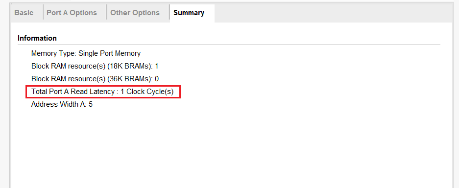
Primitives Output Register ,打开BRAM内部位于输出数据总线之后的输出流水线寄存器。
一般设计中为了改善时序性能会勾选此选项,但是会使得BRAM输出的数据延迟一拍。
数据输出总线负载多,可能带来难以满足的时序路径
-
-
Port A Output Reset Options : RAM 复位信号选项。
-
-
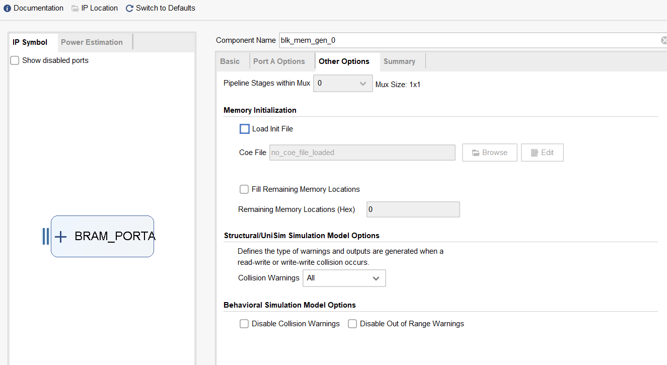
Other Options 设置RAM的初始值
RAM IP核仿真
.veo 文件是IP核自动生成的只读verilog例化模板文件。
文件1 ram_wr.v
产生读写RAM的信号, 写入32个数,再读出32个数
`timescale 1ns / 1ns
//
// Engineer: wkk
//
// Create Date: 2023/03/20 16:18:49
// Design Name:
// Module Name: ram_wr
//

module ram_wr(
    input           i_clk                           ,
    input           i_rst_n                         ,
    input           i_en                            ,
    output          o_wr_mode                       ,
    output [4:0]    o_wr_addr                       ,
    output [7:0]    o_w_data
);

reg [5:0]           cnt                            ;
reg [5:0]           cnt_reg                        ;
reg                 wr_mode_reg                    ;
//reg [7:0]           o_w_data_reg                  ;

assign o_w_data = {2'b0,cnt}                        ;
assign o_wr_addr = cnt_reg[4:0]                     ;

always @(posedge i_clk or negedge i_rst_n ) begin
    if( !i_rst_n )begin
        cnt_reg <= 6'b0;
    end else
        cnt_reg <= cnt;
end

always @(posedge i_clk or negedge i_rst_n ) begin
    if( !i_rst_n )begin
        cnt <= 6'b0;
    end
    else if(i_en) begin
        if( cnt == 6'd63 )
            cnt <= 6'b0;
        else
            cnt <= cnt + 1'b1;
    end else begin
        cnt <= 6'b0 ;
    end
end

assign o_wr_mode = wr_mode_reg;
always @(posedge i_clk or negedge i_rst_n ) begin
    if( !i_rst_n )
        wr_mode_reg <= 1'b0;                    // default read mode
    else if(i_en && cnt <= 6'd30 )
        wr_mode_reg <= 1'b1;
    else
        wr_mode_reg <= 1'b0;
end

endmodule
文件2 ram_test_top.v
进行ram读写
`timescale 1ns / 1ns
//
// Engineer: wkk
//
// Create Date: 2023/03/20 16:55:18
// Design Name:
// Module Name: ram_test_top
//

module ram_test_top(
    input           i_clk                           ,
    input           i_rst_n                         ,
    output [7:0]    o_r_data
);

//reg                         i_en                    ;
wire                        o_wr_mode               ;
wire [4:0]                  o_wr_addr               ;
wire [7:0]                  o_w_data                ;

ram_wr ram_wr_inst(
        .i_clk                              (  i_clk       ),
        .i_rst_n                            (  i_rst_n     ),
        .i_en                               (  1'b1        ),
        .o_wr_mode                          (  o_wr_mode   ),
        .o_wr_addr                          (  o_wr_addr   ),
        .o_w_data                           (  o_w_data    )
);

singleport_ram_8x32 singleport_ram_8x32_inst (
  .clka         (i_clk       ),    // input wire clka
  .wea          (o_wr_mode        ),      // input wire [0 : 0] wea
  .addra        (o_wr_addr      ),  // input wire [4 : 0] addra
  .dina         (o_w_data       ),    // input wire [7 : 0] dina
  .douta        (o_r_data      )  // output wire [7 : 0] douta
);
endmodule
文件3 ram_test_top_tb.v
`timescale 1ns / 1ns
//
// Engineer:  wkk
//
// Create Date: 2023/03/22 23:00:02
// Design Name:
// Module Name: ram_test_top_tb
//

module ram_test_top_tb();
 reg           i_clk        ;
 reg           i_rst_n      ;
 wire [7:0]    o_r_data     ;


ram_test_top ram_test_top_inst(
  .i_clk                         (i_clk   ) ,
  .i_rst_n                       (i_rst_n ) ,
  .o_r_data                      (o_r_data)
);

initial begin
    i_clk = 1'b0;
    i_rst_n = 1'b0;
    forever #5 i_clk = ~i_clk;
end

initial begin
    #10 i_rst_n = 1'b1;
    #1000 $stop;
end

endmodule
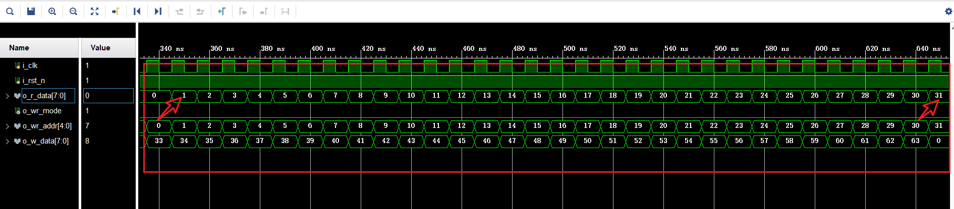
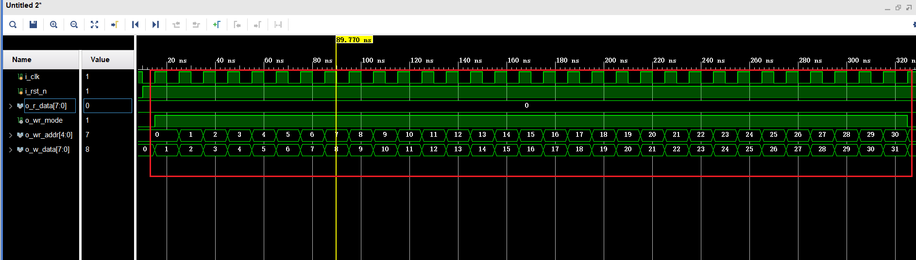
仿真结果
-
写数据,写入1-31
-
读数据,读出1-31
RAM 中读出的数据在延时一个时钟周期之后,开始输出数据