Reference: About LVDS level
High speed digital logic level (8) of LVDS
LVDS (Low-Voltage Differential Signaling, Low Voltage Differential Signaling ) is in the National Semiconductor 1994 A signal level criteria proposed in transmission mode, which uses high-speed low voltage swing differential transmission of data, point to point, or may be achieved a multipoint connection; LVDS technical specification has two standards, i.e., the TIA (Telecommunication industries Alliance) / EIA (electronic industries Alliance) in ANSI / TIA / EIA-644 standard and the IEEE 1596.3 standard, the LVDS interface is also referred to as RS -644 interface.
A, LVDS works
LVDS typical operating principle of FIG. 1 , which mainly consists of two parts driver and receiver. LVDS is driven by a drive source composed of the differential pair and the current, current sources typically 3.5mA ; LVDS receiver having a high input impedance, so most of the current driver output flow through 100Ω resistor, and the receiver generating input of approximately 350mV voltage; when the inverted level of the drive, the direction of current flowing through the resistor is changed, thus producing a corresponding output of the logic "1" and logic "0" state.
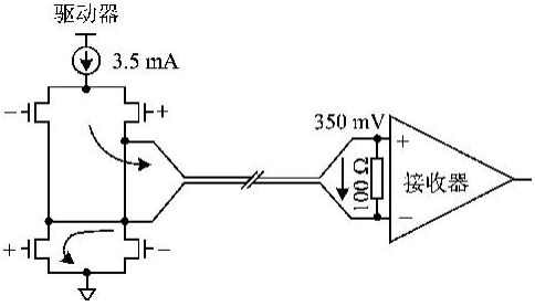
Figure 1 LVDS level circuit diagram works
Two, the LVDS advantages
2.1, high-speed transmission capability
LVDS technology constant current source mode and low mean output swing LVDS high speed driving, high-speed signal transmission; the ANSI / the TIA / EIA-644 standard recommends LVDS maximum data transfer rate of 655Mb / s and distortion on the channel theoretical limit rate 1.923Gb / S .
2.2, a low noise / low electromagnetic interference
It is well known differential data transmission mode data transmission-line common-mode noise than a stronger resistance, the two differential signal lines, current direction opposite to the voltage amplitude, and the receiver only care about the difference of the two signals, so to common mode noise coupled to form a differential line can be canceled, while the electromagnetic field around the two signal lines are also offset each other, thus the transmission ratio of the differential signal TTL electromagnetic radiation is much smaller single-ended signaling; and LVDS signal constant current source mode drive, not prone to ringing and switching spikes, further reducing noise.
2.3, low power consumption
LVDS devices generally use CMOS processes to realize, so too has a lower static power consumption, and LVDS load ( 100 [Omega] Power terminal resistor) is only 1.2mW ; while LVDS constant current source mode driving scheme greatly reduces the frequency component impact on power consumption.
2.4, Low Voltage
LVDS interface uses low voltage differential signaling technology, which does not depend on the transmission and reception of the supply voltage, so LVDS can be relatively easily applied to a low-voltage system, such as 3.3V or even 2.5V , and maintain the same level and the performance of the signal.
Three, LVDS application mode
1. The one-way point, which is a typical application mode.
2. The two-way point, by a twisted pair two-way half-duplex communication (data transfer differential signal still only one direction at any time), by a standard LVDS constituting the driver and the receiver, as shown in FIG 2 shown ; however, a better approach is to use bus LVDS driver, i.e. BLVDS , which is connected to the load bus ends are designed.
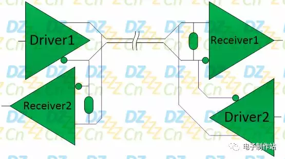
FIG 2 bidirectional LVDS circuit
3. The multi-branch form, i.e., a plurality of receivers connected to the drive. When the same data to be transmitted to a plurality of loads, such application forms.
4. The multi-point structure, a plurality of support case multipoint bus drivers, may be employed BLVDS drive, it can provide two-way half-duplex communication, but at any one time, only one drive work, and thus the transmission priority bus arbitration agreement need according to different applications use different software protocols and hardware solutions.
Four, the LVDS signal layout considerations (general high-speed signal)
1, the use of multilayer layout
LVDS signals belonging to the high-speed signal, the formation when the adjacent layers should layout, in order to achieve LVDS signal shielding to prevent interference.
2, wherein the impedance matching
LVDS voltage swing signal is only 350mV , differential signaling current driving operation, to protect them from the reflected signal which propagates in the transmission line, LVDS signals require transmission line impedance, typically differential impedance (100 ± 10) [Omega] , impedance control a direct impact on signal integrity and delay.
3、紧耦合原则
在计算线宽和差分线间距时最好遵守紧耦合的原则,也就是差分对线间距小于或等于线宽;当两条差分信号线距离很近时,电流传输方向相反,其产生的磁场相互抵消,电场相互耦合,电磁辐射也要小得多。
4、走短线、直线
为确保信号的质量,LVDS差分对走线应该尽可能短而直,减少布线中的过孔数,避免差分对布线太长(同时布线太长也会占用更多的PCB板面积),出现太多的拐弯,拐弯处尽量用45°或者弧线,避免90°拐弯。
5、不同差分线对间的处理
对于不同差分线之间的间距要求间隔不能太少,至少应大于3~5倍差分对间距,必要时在不同的差分线对之间加地孔隔离以防止相互之间的串扰。
6、高速信号应远离其他信号
对高速信号和其他信号比如TTL信号,最好使用不同的走线层,如果因为设计限制必须使用同一层走线,应保证高速信号和其他信号的距离至少大于3~5倍差分线间距。
7、高速信号尽量不跨平面分割
高速信号跨分割部分的传输线会因为缺少参考平面而导致阻抗的不连续,从而引起信号反射等现象。
8、匹配电阻的精度要求
For point to point topology, impedance cabling normal control in 100 [Omega] , but the matching resistor may be adjusted according to the actual situation, the precision resistor is preferably 1% to 2% , as a rule of thumb, 10% of the impedance mismatch will have a 5% of reflection (refer to knowledge of the impedance matching hardware design - Detailed characteristic impedance ) .