The initialization of PLL1 and 8-channel PFD has been completed previously. As for other PLL channels, it is not too late to initialize them when actually needed. Next we will select several specific peripheral clocks for configuration.
Suppose we want to initialize the following two root clocks PERCLK_CLK_ROOT and IPG_CLK_ROOT . (The root clock AHB_CLK_ROOT may also be involved in the process )
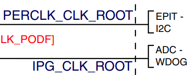
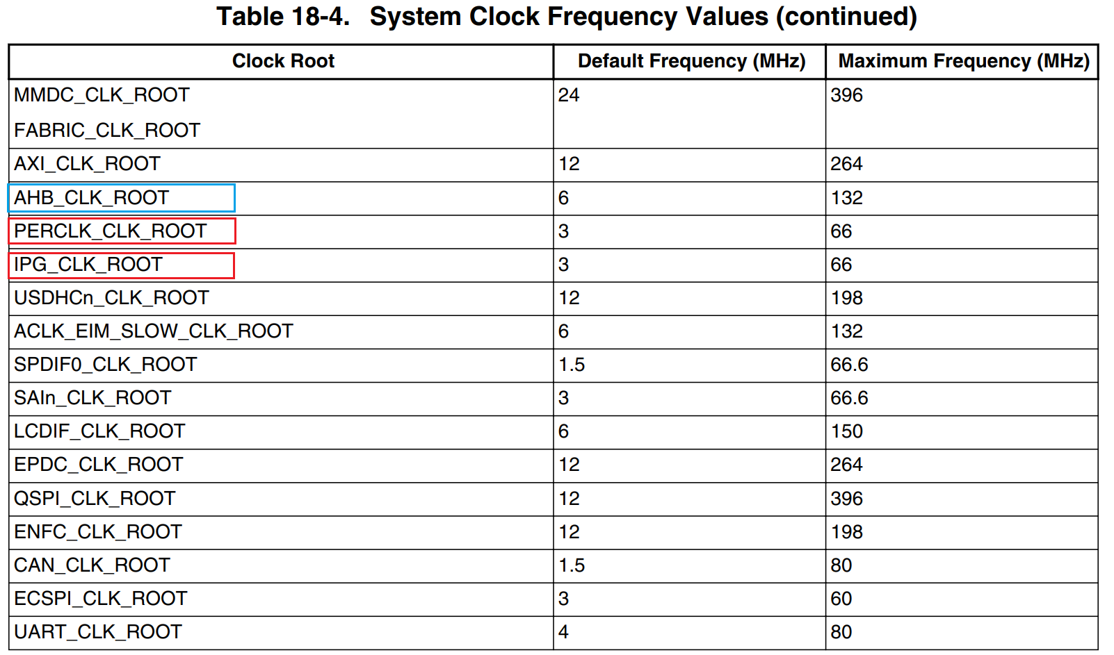
Table of contents
1. PERCLK_CLK_ROOT route analysis
2. IPG_CLK_ROOT route analysis
3. AHB_CLK_ROOT route analysis
1. AHB_CLK_ROOT route register analysis
(1) PRE_PERIPH_CLK_SEL bit of CBCMR register
(2) PERIPH_CLK_SEL bit of CBCDR register
2. IPG_CLK_ROOT route register analysis
3. PERCLK_CLK_ROOT route register analysis
1. Route selection
1. PERCLK_CLK_ROOT route analysis
There are two clock sources for PERCLK_CLK_ROOT, one is directly from the crystal oscillator OSC, and the other is from IPG_CLK_ROOT. Which one is selected is determined by the PERCLK_CLK_SEL bit of the CSCMR1 register, and the number of divisions is determined by the PERCLK_PODF bit. (What we actually did was "Choice 2")
The configuration steps are as follows:
- The first step is to set the PERCLK_CLK_SEL bit of the CSCMR1 register and select the clock source IPG_CLK_ROOT
- The second step is to set the PERCLK_PODF bit of the CSCMR1 register to divide by 1
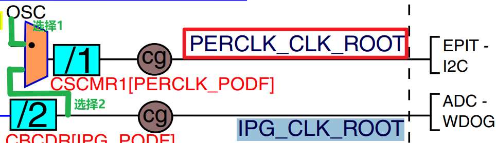
2. IPG_CLK_ROOT route analysis
There is only one clock source for IPG_CLK_ROOT, which comes from the AHB_CLK_ROOT above, one after another, so the next key is to analyze the clock source of AHB_CLK_ROOT.
The configuration steps are as follows:
- Just set the IPG_PODF bit of the CBCDR register to divide by 2
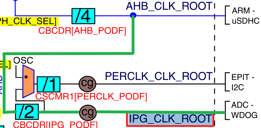
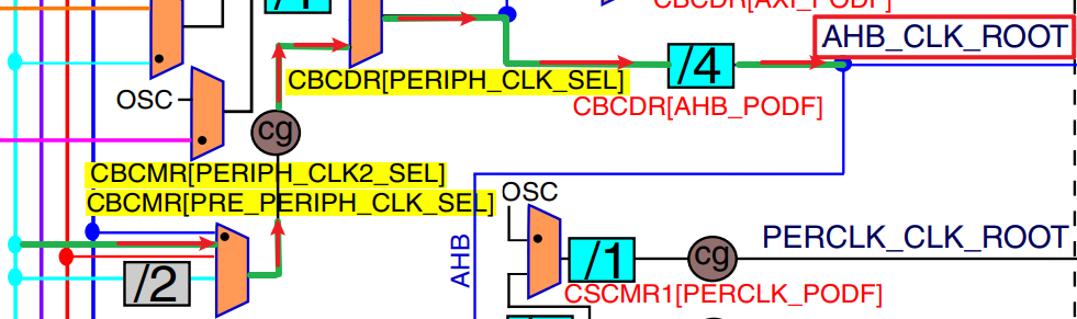
3. AHB_CLK_ROOT route analysis
According to the order of the arrows, the configuration steps are as follows:
- Set the PRE_PERIPH_CLK_SEL bit of the CBCMR register to select the PLL2_PFD2 clock source
- Set the PERIPH_CLK_SEL bit of the CBCDR register and choose the route below
Note: The AHB_PODF bit of CBCDR was originally set. Although the CBCDR written here is divided by 4, the internal boot rom has been initialized to divide by 3, so this step does not need to be done.
2. Register analysis
1. AHB_CLK_ROOT route register analysis
What you need to do in this step is:
- Set the PRE_PERIPH_CLK_SEL bit of the CBCMR register to select the PLL2_PFD2 clock source
- Set the PERIPH_CLK_SEL bit of the CBCDR register to 0
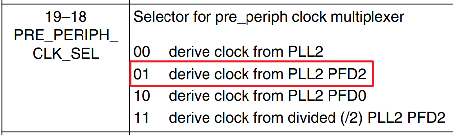
(1) PRE_PERIPH_CLK_SEL bit of CBCMR register
We first find the PRE_PERIPH_CLK_SEL bit of the CBCMR register and set it to 01.
(2) PERIPH_CLK_SEL bit of CBCDR register
Then the PERIPH_CLK_SEL bit of the CBCDR register is set to 0. This needs to be viewed with the bus design diagram (functional description in Chapter 18)
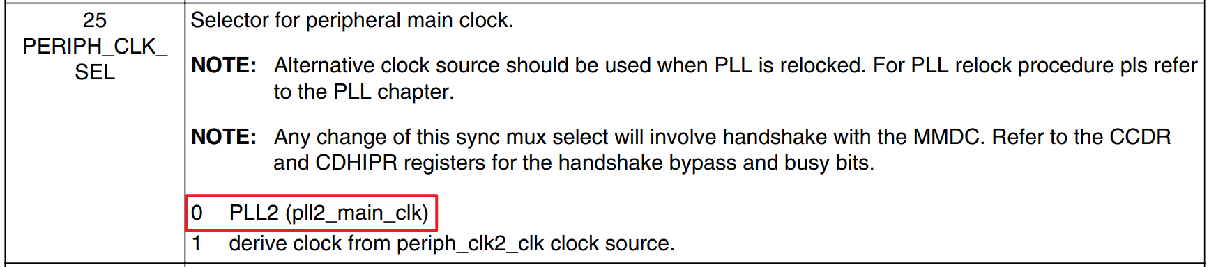

We also need to pay attention to the second prompt message (NOTE) of the PERIPH_CLK_SEL bit. No matter which choice is made, it will involve handshake with MMDC. This needs to refer to the handshake bypass and busy fields of the CCDR and CDHIPR registers.
MMDC_CH0_MASK bit of CCDR
Any change involving the mmdc_ch0_axi_podf field or periph_clk_sel field requires modifying the following field, whether to allow handshakes or block handshakes. Obviously select allow, the MMDC_CH0_MASK bit is set to 0.

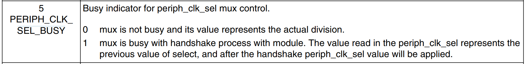
PERIPH_CLK_SEL_BUSY bit of CDHIPR
Determine whether PERIPH_CLK_SEL is processing the selection event of other selectors.
- 0: If in idle state, the selection of the PERIPH_CLK_SEL bit of the CBCDR register can be processed
- 1: If it is busy, it means you need to wait for the previous selector to end.
(3) Summary
寄存器: CCM_CBCMR
基地址: 0x20C4018
初始化操作:
    CCM_CBCMR &= ~(3 << 18);    // 19-18 位清零
    CCM_CBCMR |= (1 << 18);     // 19-18 设为01

/*
 * 在操作CCM_CBCDR之前需要做两步:
 *     1、允许和MMDC握手               —— CCDR 寄存器
 *     2、检查 PERIPH_CLK_SEL 是否忙线 —— CDHIPR 寄存器
 *
 * 做完上述两步以后才是操作 CCM_CBCDR 寄存器
 */
寄存器: CCM_CCDR
基地址: 0x20C4004
初始化操作:
    CCM_CCDR &= ~(1 << 17);    // 第 17 位置0

寄存器: CCM_CDHIPR
基地址: 0x20C4048
初始化操作:
    while((CCM_CDHIPR >> 5) & 0x01 != 0);    // 为 0 时表示空闲,跳出循环

寄存器: CCM_CBCDR
基地址: 0x20C4014
初始化操作:
    CCM_CBCDR &= ~(1 << 25);            // 第 25 位设为0
2. IPG_CLK_ROOT route register analysis
This step is relatively simple. You only need to find the IPG_PODF bit of the CBCDR register and set it to divide by 2.
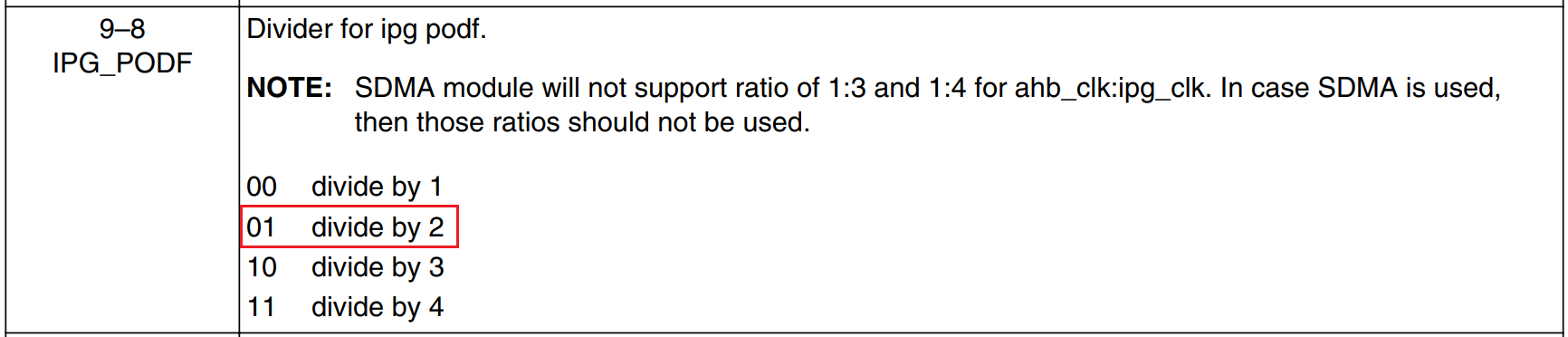
寄存器: CCM_CBCDR
基地址: 0x20C4014
初始化操作:
    CCM_CBCDR &= ~(3 << 8);    // 9-8 位清零
    CCM_CBCDR |= (1 << 8);     // 9-8 设为01
3. PERCLK_CLK_ROOT route register analysis
What you need to do in this step is:
- The first step is to set the PERCLK_CLK_SEL bit of the CSCMR1 register and select the clock source IPG_CLK_ROOT
- The second step is to set the PERCLK_PODF bit of the CSCMR1 register to divide by 1
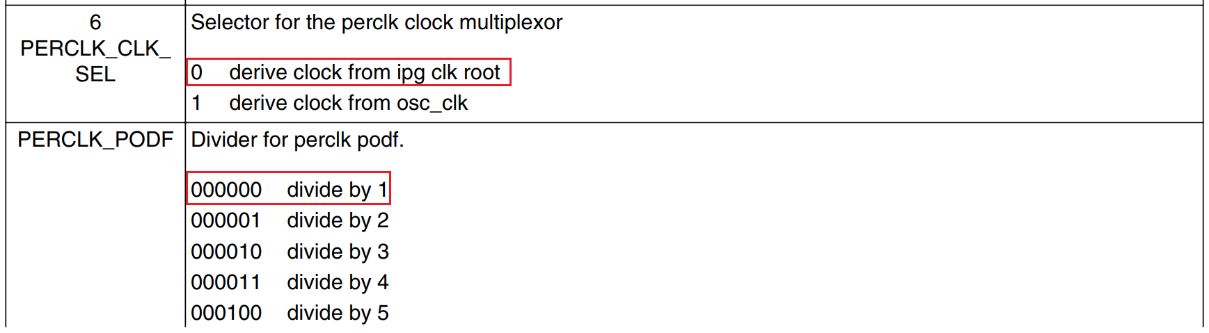
寄存器: CCM_CSCMR1
基地址: 0x20C401C
初始化操作:
    CCM_CSCMR1 &= ~(0x7F);    // 6-0 位清零