Table of contents
2. IO multiplexing as UART register analysis
3. Analysis of UART related registers
1. Understanding UART
1. Concept
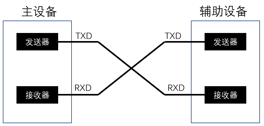
UART is a general-purpose serial and asynchronous communication bus. The bus has two data lines, TXD is used to send data, and RXD is used to receive data. It can realize full-duplex sending and receiving. It is often used in embedded systems Communication between host and auxiliary device.
2. Frame format
The UART frame format is as follows:
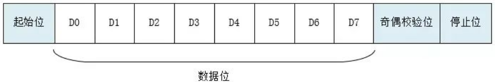
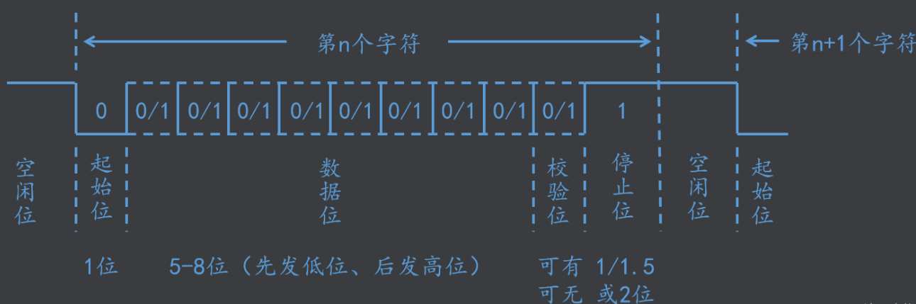
Idle bit: no data transmission (maintained at high level by default)
Start bit: Indicates that data is about to be sent, and it will become low at this time
Data bits: Generally, there are 8 bits, which represent a byte.
Check digit: It is convenient for the receiver to check whether the data has been tampered with (optional)
Stop bit: Indicates the end of a frame of data. It is equivalent to inform the other party that the data has been sent and return to the high level (idle state)
2. IO multiplexing as UART register analysis
Since IO is involved, it is necessary to consider configuring pins to be multiplexed as UART functions.
1. Schematic analysis
First find the USB USART module in the schematic diagram of the baseboard, and now there are more USB interfaces on the computer, so many serial TTL-to-USB chips (such as CH340, PL2303) have been produced.
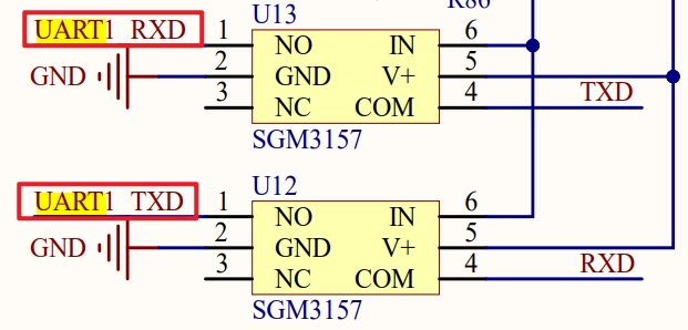
Then we go to the core board to find out which two pins of the core board UART1_RXD and UART1_TXD are connected to.
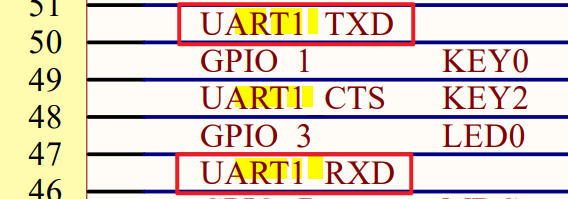
Therefore, we need to find the registers related to UART1 and TXD and RXD.
2. Register analysis
Since it involves pin multiplexing, it involves multiplexing configuration and electrical property configuration.
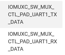
- I/O multiplexing
- IOMUXC_SW_MUX_CTL_PAD_UART1_TX_DATA
- IOMUXC_SW_MUX_CTL_PAD_UART1_RX_DATA
![]()
![]()
- Configure Electrical Properties
- IOMUXC_SW_PAD_CTL_PAD_UART1_TX_DATA
- IOMUXC_SW_PAD_CTL_PAD_UART1_RX_DATA
/************ 配置 IO 复用 **********/
寄存器: IOMUXC_SW_MUX_CTL_PAD_UART1_TX_DATA
基地址: 0x20E0084
初始化操作:
    IOMUXC_SW_MUX_CTL_PAD_UART1_TX_DATA &= ~(0xF);

寄存器: IOMUXC_SW_MUX_CTL_PAD_UART1_RX_DATA
基地址: 0x20E0088
初始化操作:
    IOMUXC_SW_MUX_CTL_PAD_UART1_RX_DATA &= ~(0xF);

/************ 配置电气属性 **********/
// 主要参考之前 LED 的电气属性配置
寄存器: IOMUXC_SW_PAD_CTL_PAD_UART1_TX_DATA
基地址: 0x20E0310
初始化操作:
    IOMUXC_SW_MUX_CTL_PAD_UART1_TX_DATA = 0x10B0;

寄存器: IOMUXC_SW_PAD_CTL_PAD_UART1_RX_DATA
基地址: 0x20E0314
初始化操作:
    IOMUXC_SW_PAD_CTL_PAD_UART1_RX_DATA = 0x10B0;
Electrical attribute configuration reference: LED driver register analysis
3. Analysis of UART related registers
The following are the registers related to UART initialization:
- UARTx_UCR1~4: Serial port configuration registers. Serial port enable, number of data bits, number of stop bits, etc.
- UARTx_USR1~2: Serial port status register. It can be used to judge whether the data is received, whether the data is sent, etc.
- UARTx_UFCR, UARTx_UBIR , UARTx_UBMR: used together to configure the baud rate
Registers related to UART practical application:
- UARTx_URXD: Save the received data, whether there is an error in the reception, etc.
- UARTx_UTXD: save data for sending
1、UART1_UCR1~4
UARTx_UCR1:
① bit 0: UART off/enable. (0: disable 1: enable)
② bit 14: Auto-detect baud rate enable. It is set to disable here, because we will manually set the baud rate through the register later
![]()
UARTx_UCR2:
① bit 0: Soft reset. Reset the transmitter, receiver, all FIFOs and related registers.
![]()
② bit 1: receiver enable (receive data enable. 0: disable 1: enable)
③ bit 2: Transmitter enable (enable sending data. 0: disable 1: enable)
④ bit 5: Set the length of the data bit (excluding the start bit, stop bit, parity bit. 0: The data bit is 7 bits 1: The data bit is 8 bits)
⑤ bit 6: Set the stop bit length (0: 1 stop bit 1: 2 stop bits)
⑥ bit 7: Set parity check (0: even check 1: odd check)
⑦ bit 8: check enable (0: disable 1: enable)
⑧ bit 14: whether to ignore the RTS pin (0: use the RTS pin 1: ignore the RTS pin)
UARTx_UCR3:
① bit 2: Multiplexing selection. If the UART is multiplexed by a certain pin, then this bit needs to be set to 1
![]()
UARTx_UCR4 (no bits to configure)
寄存器: UART1_UCR1
基地址: 0x2020080
初始化操作:
    /*
     * bit 0: 0 初始禁止(等其他寄存器配置完了再使能)
     * bit 14: 0 禁止自动检测波特率
     */
    UART1_UCR1 &= ~(1 << 0);
    UART1_UCR1 &= ~(1 << 14);

寄存器: UART1_UCR2
基地址: 0x2020084
初始化操作:
    /*
     * bit 0: 0 软复位(放在其他配置之前,等待软复位结束再配置其他寄存器)
     * bit 1: 1 接收使能
     * bit 2: 1 发送使能
     * bit 5: 1 数据位为 8 bit
     * bit 6: 0 停止位占 1 bit
     * bit 8: 0 关闭奇偶校验
     * bit 14: 1 无视RTS引脚(无需硬件流控)
     */
    UART1_UCR2 &= ~(1 << 0);
    while((UART1_UCR2 & 0x01) == 0);    // 等待软复位结束
    UART1_UCR2 |= ((1 << 1) | (1 << 2) | (1 << 5) | (1 << 14));
    UART1_UCR2 &= ~((1 << 6) | (1 << 8));

寄存器: UART1_UCR3
基地址: 0x2020088
初始化操作:
    UART1_UCR3 |= (1 << 2);        // 只要被复用为 UART1 功能,该位需置1

寄存器: UART1_UCR4
基地址: 0x202008C
2、UART1_USR1~2
Here we mainly focus on bit 0 and bit 3 in UARTx_USR2
- bit 0: Is data ready (whether data is received)
- bit 3: Whether the data has been sent
寄存器: UART1_USR2
基地址: 0x2020098
3. Baud rate configuration
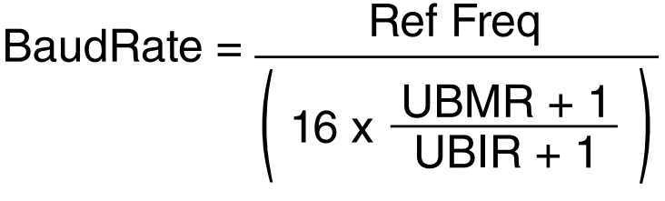
The formula for calculating the baud rate is as follows. It mainly involves the following three registers, which we mainly set are:
- UARTx_UFCR: Set the frequency division of uart clock.
- UARTx_UBIR:bit 15-0
- UARTx_UBMR:bit 15-0
(1) Ref Freq
The clock source of UART comes from the system clock PLL3 (480MHz). After dividing by 6 and 1, the obtained uart_clk = 80MHz.
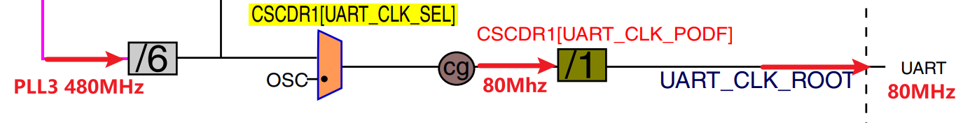
The frequency can be divided again inside the UART, and the final result is Ref Freq

(2) Register configuration
Assume that the baud rate we want to set is 115200, and there is no internal frequency division ( UARTx_UFCR = 1 ), so the next thing to determine is UBMR and UBIR. The answer is announced directly, the number is made up.
- UARTx_UFCR = 1
- UBIR = 71
- UBMR = 3124
寄存器: UART1_UFCR
基地址: 0x2020090
初始化操作:
    /*
     * bit 9-7: 101 分频数为1
     */
    UART1_UFCR &= ~(7 << 7);
    UART1_UFCR |= (5 << 7);

寄存器: UART1_UBIR
基地址: 0x20200A4
初始化操作:
    UART1_UBIR = 0;
    UART1_UBIR = 71;

寄存器: UART1_UBMR
基地址: 0x20200A8
初始化操作:
    UART1_UBMR = 0;
    UART1_UBMR = 3124;
4、UART1_URXD
寄存器: UART1_URXD
基地址: 0x2020000
获取接收数据: UART1_URXD & 0xFF
5、UART1_UTXD
寄存器: UART1_UTXD
基地址: 0x2020040
设置发送内容:
    UART1_UTXD &= ~0xFF;        // 低 8 位清零
    UART1_UTXD |= val;          // val 表示要填入的发送内容