i2c_bit_shift
The module block diagram is as follows.
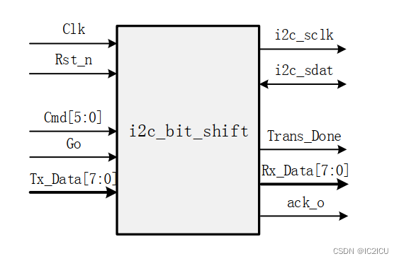
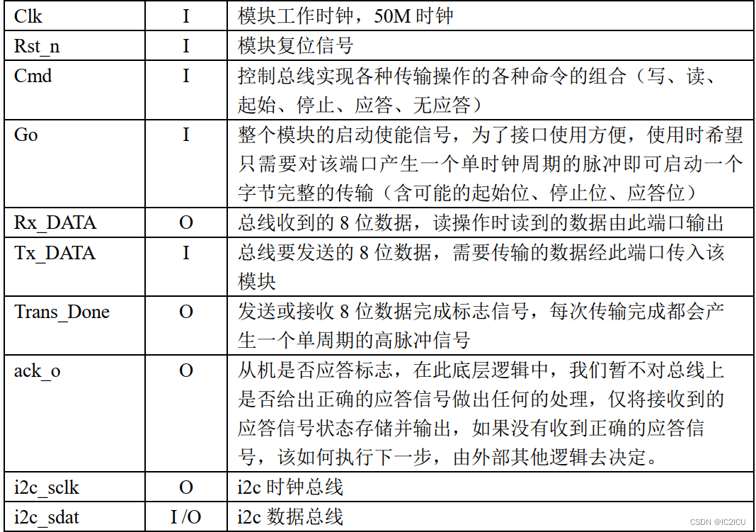
Input and output signals:
The overall idea is as follows:
through the combination of input commands, an 8-byte data transmission is completed. 6 commands are defined,
| WR | Write Data Request (6'b000_001) |
|---|---|
| STA | Start bit request (6'b000_010) |
| RD | Read data request (6'b000_100) |
| STO | Stop bit request (6'b001_000) |
| ACK | Acknowledgment bit request (6'b010_000) |
| NACK | No response to request (6'b100_000) |
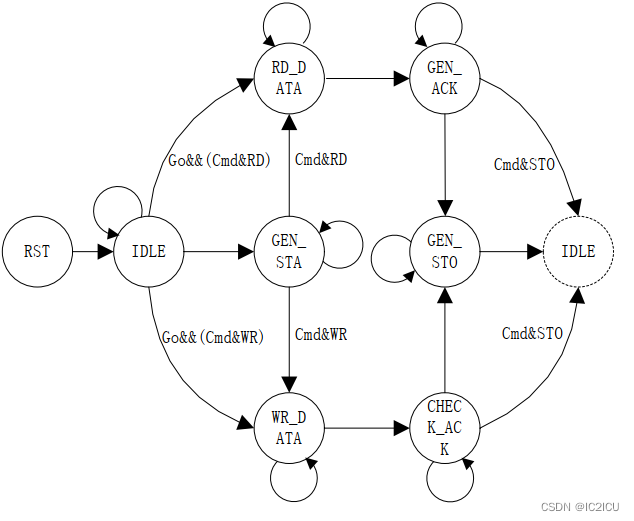
The idea of applying a sequence machine in a state machine is adopted. Each state is divided into four steps to complete the transmission of one bit of data, and is controlled by a counter. The defined state is as follows (one-hot encoding):
| state | description |
|---|---|
| IDLE | idle state |
| GEN_STA | generate start signal |
| WR_DATA | Write data status |
| RD_DATA | Read data status |
| CHECK_ACK | Detect response signal |
| GEN_ACK | generate response signal |
| GNE_STO | generate stop signal |
The state machine transitions look like this:
The code is as follows, with very clear comments:
module i2c_bit_shift (
input wire clk ,
input wire rst_n ,
input wire [5:0] cmd , //控制总线实现各种传输的各种命令组合
input wire go , //整个模块的启动信号
input wire [7:0] Tx_Data , //总线要发送的8位数据
output reg i2c_sclk , //i2c时钟总线
inout wire i2c_sdat , //i2c数据总线
output reg Trans_Done , //传输完成信号
output reg [7:0] Rx_Data , //总线要接收的8位数据
output reg ack_o //从机时候应答标志
);
localparam IDLE = 7'b0000_001, //空闲状态
GEN_STA = 7'b0000_010, //产生起始信号
WR_DATA = 7'b0000_100, //写数据状态
RD_DATA = 7'b0001_000, //读数据状态
CHECK_ACK = 7'b0010_000, //检测应答信号
GEN_ACK = 7'b0100_000, //产生应答信号
GNE_STO = 7'b1000_000; //产生停止信号
localparam WR = 6'b000_001, //写数据请求
STA = 6'b000_010, //起始位请求
RD = 6'b000_100, //读数据请求
STO = 6'b001_000, //停止位请求
ACK = 6'b010_000, //应答位请求
NACK = 6'b100_000; //无应答请求
parameter SYS_CLOCK = 50_000_000; //系统采用50MHz时钟
parameter SCL_CLOCK = 400_000 ; //SCL总线时钟采用400khz
localparam SCL_CNT_M = SYS_CLOCK / SCL_CLOCK / 4 - 1; //产生时钟SCL计数器最大值
reg en_div_cnt ; //计数器使能信号
reg i2c_sda_oe ; //三态门使能信号,1:输出,0:输入
reg [6:0] state ; //状态机的状态变量
reg [5:0] cnt ; //计数器
reg i2c_sdat_o ; //输出的i2c_sdat_o
reg [19:0] div_cnt ; //分频信号
wire sclk_plus = (div_cnt == SCL_CNT_M); //dic_cnt计数到最大值产生一个高脉冲
//reset为低时,若干信号的初始化
always @(posedge clk or negedge rst_n) begin
if(!rst_n) begin
en_div_cnt <= 1'b0;
i2c_sda_oe <= 1'b1;
state <= IDLE;
cnt <= 0;
i2c_sdat_o <= 1'b0;
i2c_sclk <= 1'b1;
Rx_Data <= 8'd0;
end
end
//一段式状态机
always @(posedge clk or negedge rst_n) begin
case(state)
IDLE: begin
Trans_Done <= 1'b0;
i2c_sda_oe <= 1'b1;
if(go) begin //整个模块的启动信号go
en_div_cnt <= 1'b1; //使能div_cnt计数器,跳转的状态都需要这个计数器
if(cmd & STA ) //起始命令
state <= GEN_STA; //跳转到起始状态
else if(cmd & WR) //写命令
state <= WR_DATA; //跳转到写数据状态
else if(cmd & RD) //读命令
state <= RD_DATA; //跳转到读数据状态
else
state <= IDLE; //都不满足则跳转到IDLE状态
end
else begin
en_div_cnt <= 1'b0; //模块未启动
state <= IDLE; //跳转到IDLE状态,且不使能div_cnt计数器
end
end
GEN_STA:begin //i2c_sclk为高电平时,i2c_sda从高电平变成低电平产生起始位
if(sclk_plus) begin //只有在sclk_plus产生高脉冲的时候,div_cnt计数到最大值
if(cnt == 3) //cnt计数到3,归0
cnt <= 0;
else
cnt <= cnt + 1'b1; //否则计数器自增1
case(cnt) //分四步
0:begin i2c_sdat_o <= 1'b1; i2c_sda_oe <= 1'b1; end //cnt为0时,i2c_sdat_o拉高,三态门输出
1:begin i2c_sclk <= 1'b1; end //cnt为1时,拉高i2c_sclk
2:begin i2c_sdat_o <= 0; i2c_sclk <= 1; end //cnt为2时,继续拉高i2c_sclk,拉低i2c_sdat_o
3:begin i2c_sclk <= 0; end //cnt为3时,拉低i2c_sclk
default: begin i2c_sdat_o <= 1'b1; i2c_sclk <= 1'b1; end
endcase
if(cnt == 3) begin
if(cmd & WR)
state <= WR_DATA; //跳转到写数据状态
else if(cmd & RD)
state <= RD_DATA; //跳转到读数据状态
end
end
end
WR_DATA:begin //写数据时,只有在sclk为低电平的时候,sda才可以变化
if(sclk_plus) begin //8位数据,每位数据分4步,故cnt计数器计数到31
if(cnt == 31)
cnt <= 0;
else
cnt <= cnt + 1'b1;
case(cnt)
0,4,8,12,16,20,24,28:
begin
i2c_sdat_o <= Tx_Data[7-cnt[4:2]]; //在GNE_STA状态时,i2c_sclk拉低了,所以此时把Tx_data一位传给i2s_sdat_o
i2c_sda_oe <= 1'b1; //三态门输出使能
end
1,5,9,13,17,21,25,29:
begin
i2c_sclk <= 1'b1; //sclk posedge 拉高i2c_sclk
end
2,6,10,14,18,22,26,30:
begin
i2c_sclk <= 1'b1; //sclk keep high 继续拉高i2c_sclk
end
3,7,11,15,19,23,27,31:
begin
i2c_sclk <= 1'b0; //sclk negedge 拉低i2c_sclk,以便在下次传输Tx_Data的一位
end
default: begin i2c_sdat_o <= 1; i2c_sclk <= 1; end
endcase
if(cnt == 31) begin
state <= CHECK_ACK; //Tx_Data的8位写完之后,跳转到检查应答位状态
end
end
end
CHECK_ACK:begin
if(sclk_plus) begin
if(cnt == 3)
cnt <= 0;
else
cnt <= cnt + 1;
case(cnt) //应答位的检查依然分四步完成,使用计数器cnt来控制
0: begin i2c_sda_oe <= 1'b0; i2c_sclk <= 1'b0; end //拉低i2c_sclk信号,并且设置三态门为输入
1: begin i2c_sclk <= 1; end //拉高i2c_sclk
2: begin ack_o <= i2c_sdat; i2c_sclk <= 1; end //拉高i2c_sclk,并且把i2c_sdat赋值给ack_o,
3: begin i2c_sclk <= 0; end //拉低i2c_sclk
default: begin i2c_sdat_o <= 1'b1; i2c_sclk <= 1'b1; end //上面连续两次拉高i2c_sclk是为了占空比为50%的i2c_sclk时钟
endcase
if(cnt == 3) begin
if(cmd & STO)
state <= GNE_STO; //跳转到产生停止位状态
else begin
state <= IDLE;
Trans_Done <= 1'b1; //一次传输完成
end
end
end
end
GNE_STO : begin //在i2c_sclk为高电平,i2c_sda从低到高则为停止信号
if(sclk_plus) begin //与产生起始信号类似
if(cnt == 3)
cnt <= 0;
else
cnt <= cnt + 1'b1;
case(cnt)
0: begin i2c_sdat_o <= 1'b0; i2c_sda_oe <= 1'b1; end //三态门输出, i2c_sda拉低
1: begin i2c_sclk <= 1'b1; end //拉高i2c_sclk
2: begin i2c_sdat_o <= 1'b1; i2c_sclk <= 1'b1; end //拉高i2c_sda,i2c_sclk
3: begin i2c_sclk <= 1'b1; end
default: begin i2c_sdat_o <= 1'b1; i2c_sclk <= 1'b1; end
endcase
if(cnt == 3) begin
Trans_Done <= 1'b1; //传输完成
state <= IDLE;
end
end
end
RD_DATA: begin //取数据
if(sclk_plus) begin
if(cnt == 31)
cnt <= 0;
else
cnt <= cnt + 1'b1; //8位,每位分4步完成
case(cnt)
0,4,8,12,16,20,24,28:
begin
i2c_sda_oe <= 1'b0;
i2c_sclk <= 0; //set data,拉低i2c_sclk,三态门设置为输入
end
1,5,9,13,17,21,25,29:
begin
i2c_sclk <= 1'b1; //sclk posedge, 拉高i2c_scclk
end
2,6,10,14,18,22,26,30:
begin
i2c_sclk <= 1'b1; //sclk keep high 利用移位的方法来存储,技巧需掌握
Rx_Data <= {
Rx_Data[6:0], i2c_sdat};
end
3,7,11,15,19,23,27,31: //sclk negedge
begin
i2c_sclk <= 1'b0;
end
default: begin i2c_sdat_o <= 1; i2c_sclk <= 1; end
endcase
if(cnt == 31) begin
state <= GEN_ACK;
end
end
end
GEN_ACK: begin //产生应答信号
if(sclk_plus) begin //分四步完成
if(cnt == 3)
cnt <= 0;
else
cnt <= cnt + 1'b1;
case(cnt)
0: begin
i2c_sda_oe <= 1'b1; //三态门输出
i2c_sclk <= 1'b0; //拉低i2c_sclk
if(cmd & ACK) //产生ACK,输出0
i2c_sdat_o <= 1'b0;
else if(cmd & NACK) //产生NOACK,输出1
i2c_sdat_o <= 1'b1;
end
1: begin i2c_sclk <= 1'b1; end
2: begin i2c_sclk <= 1'b1; end
3: begin i2c_sclk <= 1'b0; end
default: begin i2c_sdat_o <= 1; i2c_sclk <= 1; end
endcase
if(cnt == 3) begin
if(cmd & STO)
state <= GNE_STO; //跳转到产生停止位状态
else begin
state <= IDLE;
Trans_Done <= 1'b1; //传输完成
end
end
end
end
default: begin
i2c_sclk <= 1'b1;
Trans_Done <= 1'b0;
i2c_sdat_o <= 1'b0;
i2c_sda_oe <= 1'b1;
cnt <= 0;
end
endcase
end
//在en_div_cnt使能,div_cnt开始奇数,计数大最大值循环计数
always @(posedge clk or negedge rst_n) begin
if(!rst_n)
div_cnt <= 20'd0;
else if(en_div_cnt) begin
if(div_cnt < SCL_CNT_M)
div_cnt <= div_cnt + 1'b1;
else
div_cnt <= 0;
end
else
div_cnt <= 20'd0;
end
assign i2c_sdat = !i2c_sdat_o && i2c_sda_oe ? 1'b0 : 1'bz; //三态门设置
endmodule
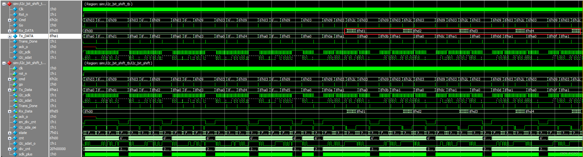
The tested tb file is as follows, writing 1, 2, 3, 4, and 5 to 0x0A, 0x0B, 0x0C, 0x0D, and 0X0F respectively. Then read them out again.
`timescale 1ns/1ns
module i2c_bit_shift_tb;

	reg Clk;
	reg Rst_n;

	reg [5:0]Cmd;
	reg Go;
	wire [7:0]Rx_DATA;
	reg [7:0]Tx_DATA;
	wire  Trans_Done;
	wire  ack_o;
	wire i2c_sclk;
	wire i2c_sdat;

	pullup PUP (i2c_sdat);

	localparam
		WR =  6'b000001,	// 写请求
		STA = 6'b000010,	//起始位请求
		RD =  6'b000100,	//读请求
		STO = 6'b001000,	//停止位请求
		ACK = 6'b010000,	//应答位请求
		NACK = 6'b100000;	//无应答请求

/*
	i2c_bit_shift i2c_bit_shift(
		.Clk(Clk),
		.Rst_n(Rst_n),
		.Cmd(Cmd),
		.Go(Go),
		.Rx_DATA(Rx_DATA),
		.Tx_DATA(Tx_DATA),
		.Trans_Done(Trans_Done),
		.ack_o(ack_o),
		.i2c_sclk(i2c_sclk),
		.i2c_sdat(i2c_sdat)
	);
*/
	i2c_bit_shift i2c_bit_shift(
		.clk(Clk),
		.rst_n(Rst_n),
		.cmd(Cmd),
		.go(Go),
		.Rx_Data(Rx_DATA),
		.Tx_Data(Tx_DATA),
		.Trans_Done(Trans_Done),
		.ack_o(ack_o),
		.i2c_sclk(i2c_sclk),
		.i2c_sdat(i2c_sdat)
	);

	M24LC04B M24LC04B(
		.A0(0),
		.A1(0),
		.A2(0),
		.WP(0),
		.SDA(i2c_sdat),
		.SCL(i2c_sclk),
		.RESET(~Rst_n)
	);

	initial Clk = 1;
	always #10 Clk = ~Clk;

	initial begin
		Rst_n = 0;
		Cmd = 0;
		Go = 0;
		Tx_DATA = 0;
		#2001;
		Rst_n = 1;
		#2000;

		write_one_byte(8'hA0,8'h0A,8'hd1);
		//#20000;
		write_one_byte(8'hA0,8'h0B,8'hd2);
		//#20000;
		write_one_byte(8'hA0,8'h0C,8'hd3);
		//#20000;
		write_one_byte(8'hA0,8'h0D,8'hd4);
		//#20000;
		write_one_byte(8'hA0,8'h0F,8'hd5);
		//#20000;

		read_one_byte(8'hA0,8'h0A);
		//#20000;
		read_one_byte(8'hA0,8'h0B);
		//#20000;
		read_one_byte(8'hA0,8'h0C);
		//#20000;
		read_one_byte(8'hA0,8'h0D);
		//#20000;
		read_one_byte(8'hA0,8'h0F);
		//#20000;
		$stop;
	end

	task write_one_byte;
		input [7:0]device_id;						//器件地址
		input [7:0]mem_address; 					//寄存器地址
		input [7:0]data;							//需要写的数据
		begin
			Cmd = WR | STA;							//写入产生起始位和写数据命令
			Go = 1;									//启动整个模块
			Tx_DATA = device_id;					//把器件地址赋值给Tx_Data
			#20;
			Go = 0;									//延迟一个时钟周期拉低go信号
			#200;
			@(posedge Trans_Done);					//等待此次传输数据完成
			#20;
			//#20000;

			Cmd = WR;								//传入写数据命令
			Go = 1;									//启动整个模块
			Tx_DATA = mem_address;					//把寄存器地址赋值给Tx_Data
			#20;
			Go = 0;									//延迟一个时钟周期拉低go信号
			#200;
			@(posedge Trans_Done);					//等待此次数据传输完成
			//#20000;
			#20

			Cmd = WR | STO;							//传入写数据和产生停止位的命令
			Go = 1;									//启动整个模块
			Tx_DATA = data;							//把需要写入的数据赋值给Tx_Data
			#20;
			Go = 0;									//延迟一个时钟周期拉低go信号
			#200;
			@(posedge Trans_Done);					//等待此次传输数据完成
			#20000;
		end
	endtask

	task read_one_byte;
		input [7:0]device_id;						//传入器件地址
		input [7:0]mem_address;						//传入寄存器地址
		begin
			Cmd = WR | STA;							//传入写数据和产生开始位的命令
			Go = 1;									//启动整个模块
			Tx_DATA = device_id;					//把器件地址赋值给Tx_Data
			#20;
			Go = 0;									//延迟一个时钟周期拉低go信号
			#200;
			@(posedge Trans_Done);					//等待此次传输数据完成
			#20000;

			Cmd = WR | STO;
			Go = 1;
			Tx_DATA = mem_address;
			#20;
			Go = 0;
			#200;
			@(posedge Trans_Done);
			//#20000;
			#20;

			Cmd = WR | STA;
			Go = 1;
			Tx_DATA = device_id | 8'd1;
			#20;
			Go = 0;
			#200;
			@(posedge Trans_Done);
			//#20000;
			#20;

			Cmd = RD | NACK | STO;
			Go = 1;
			#20;
			Go = 0;
			#200;
			@(posedge Trans_Done);
			//#20000;
			#20;
		end
	endtask


endmodule
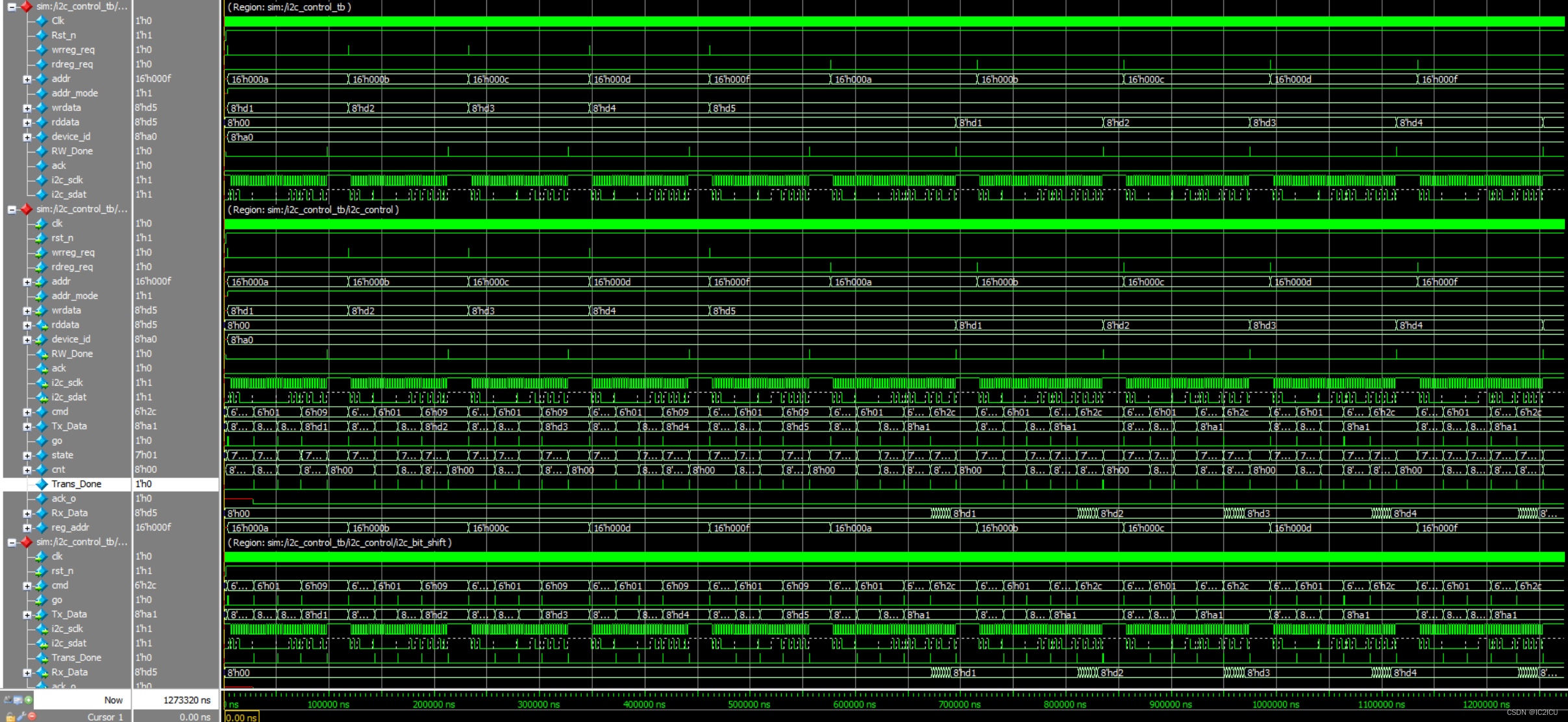
The simulation waveform is as follows, which shows that the data was successfully read:
I2C control module
Since the i2c_bit_shift module can only send one byte of data, writing input or reading output at a time requires writing several bytes. Therefore, several tasks of writing bytes can be assigned to write input and input respectively, both of which start from the IDLE state. However, these tasks are sequential and must wait for the completion of the previous task. At this time, our Trans_done signal comes in handy. Therefore, it can be designed using a state machine.
For a write-once:
for a read-once:
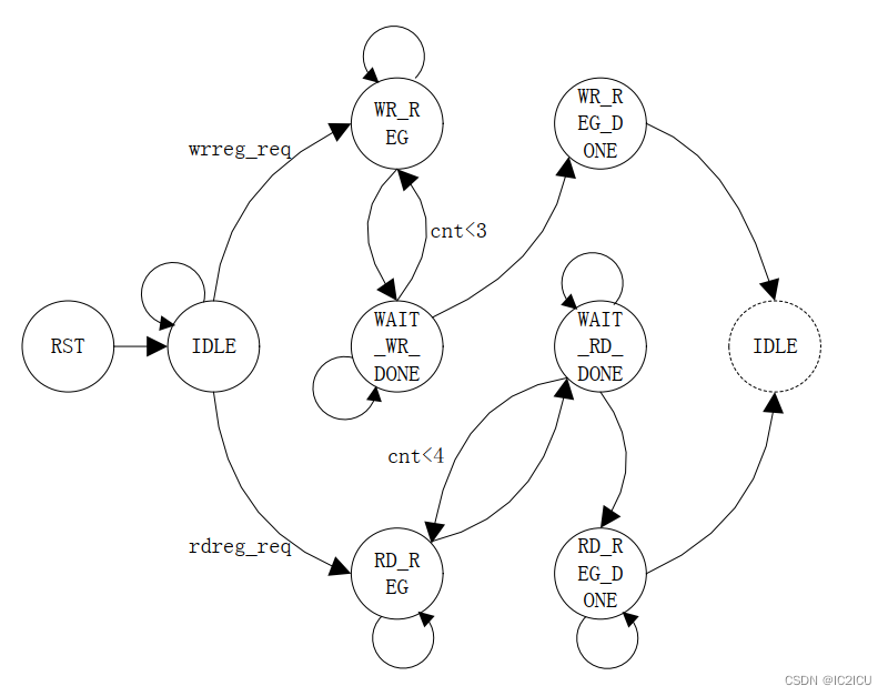
there is the following status (encoded with one-hot encoding):
| IDLE | idle state |
|---|---|
| WR_REG | write status |
| WAIT_WR_DONE | Waiting for write completion status |
| WR_REG_DONE | Write completion status |
| RD_REG | read status |
| WAIT_RD_DONE | Waiting for read completion status |
| RD_REG_DONE | read completion status |
State transition diagram:
The code of the control module is as follows (there are very detailed comments in the code), so I won’t explain it further.
module i2c_ctrl(
input wire clk , //时钟信号
input wire rst_n , //复位信号
input wire wrreg_req , //写请求信号
input wire rdreg_req , //读请求信号
input wire [15:0] addr , //16位地址输入
input wire addr_mode , //输入地址的模式,0:8位的地址 1:16位的地址
input wire [7:0] wrdata , //总线发送的8位数据
output reg [7:0] rddata , //总线接收的8位数据
input wire [7:0] device_id , //i2c器件的ID
output reg RW_Done , //读/写完成的标志
output reg ack , //从机是否应答标志
output wire i2c_sclk , //i2c时钟总线
inout wire i2c_sdat
);
localparam IDLE = 7'b0000_001, //空闲状态
WR_REG = 7'b0000_010, //写状态
WAIT_WR_DONE= 7'b0000_100, //等待写完成状态
WR_REG_DONE = 7'b0001_000, //写完成状态
RD_REG = 7'b0010_000, //读状态
WAIT_RD_DONE= 7'b0100_000, //等待读完成状态
RD_REG_DONE = 7'b1000_000; //读完成状态
localparam WR = 6'b000_001, //写数据请求
STA = 6'b000_010, //起始位请求
RD = 6'b000_100, //读数据请求
STO = 6'b001_000, //停止位请求
ACK = 6'b010_000, //应答位请求
NACK = 6'b100_000; //无应答请求
reg [5:0] cmd ;
reg [7:0] Tx_Data ;
reg go ;
reg [6:0] state ;
reg [7:0] cnt ;
//reg [15:0] reg_addr ;
wire Trans_Done ;
wire ack_o ;
wire [7:0] Rx_Data ;
wire [15:0] reg_addr ;
i2c_bit_shift i2c_bit_shift (
.clk (clk) ,
.rst_n (rst_n) ,
.cmd (cmd) ,
.go (go) ,
.Tx_Data (Tx_Data) ,
.i2c_sclk (i2c_sclk) ,
.i2c_sdat (i2c_sdat) ,
.Trans_Done (Trans_Done) ,
.Rx_Data (Rx_Data) ,
.ack_o (ack_o)
);
assign reg_addr = (addr_mode) ? addr : {
addr[7:0], addr[15:8]};
always @(posedge clk or negedge rst_n)
if(!rst_n) begin
cmd <= 6'd0;
Tx_Data <= 8'd0;
go <= 1'b0;
rddata <= 8'd0;
state <= IDLE;
ack <= 0;
end
else begin
case(state)
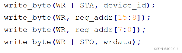
RD_REG: begin //读寄存器状态包括读数据的四个task
state <= WAIT_RD_DONE; //跳转等待读完成状态
case(cnt)
0: write_byte(WR | STA, device_id) ; //产生起始位并写入器件地址
1: write_byte(WR, reg_addr[15:8]) ; //写入寄存器地址的高8位
2: write_byte(WR, reg_addr[7:0]); //写入寄存器地址的低8位
3: write_byte(WR | STA, device_id | 8'd1); //产生起始位并写入器件地址(最后一位是1,表示读)
4: read_byte(RD | NACK | STO); //读数据并且产生NACK,STOP信号
default:;
endcase
end
WAIT_RD_DONE:begin
go <= 1'b0; //拉低go信号
if(Trans_Done) begin //等待此次数据传输完成
if(cnt <= 3)
ack <= ack | ack_o;
case(cnt)
0: begin cnt <= 1; state <= RD_REG; end //cnt为0时,cnt加1,跳转读寄存器状态
1: begin
state <= RD_REG;
if(addr_mode) //根据地址模式
cnt <= 2; //addr_more为1:16位地址
else
cnt <= 3; //addr_mode位0,8位地址
end
2: begin
cnt <= 3;
state <= RD_REG;
end
3: begin
cnt <= 4;
state <= RD_REG;
end
4: state <= RD_REG_DONE; //cnt为4时,跳转到读完成状态
default: state <= IDLE;
endcase
end
end
RD_REG_DONE:begin
RW_Done <= 1'b1; //拉高读写完成信号
rddata <= Rx_Data; //把读出的数据Rx_Data赋值给rddata
state <= IDLE; //跳转到IDLE状态
end
WR_REG: begin
state <= WAIT_WR_DONE; //跳转到等待写完成状态
case(cnt)
0: write_byte(WR | STA, device_id); //产生起始位并写入器件地址
1: write_byte(WR, reg_addr[15:8]); //写入寄存器地址的高8位
2: write_byte(WR, reg_addr[7:0]); //写入寄存器地址的低8位
3: write_byte(WR | STO, wrdata); //写入数据并且产生停止位
default:;
endcase
end
WAIT_WR_DONE:begin
go <= 1'b0; //拉低go信号
if(Trans_Done) begin //等待此次传输数据完成
ack <= ack | ack_o;
case(cnt)
0: begin cnt <= 1; state <= WR_REG; end //cnt为0时,跳转写寄存器状态
1: begin
state <= WR_REG;
if(addr_mode) //不同的地址模式
cnt <= 2; //决定时写入16位还是8位
else
cnt <= 3;
end
2: begin
cnt <= 3;
state <= WR_REG;
end
3: state <= WR_REG_DONE; //cnt为3时,跳转写完成状态
default: state <= IDLE;
endcase
end
end
WR_REG_DONE:begin
RW_Done <= 1'b1; //拉高读写完成信号
state <= IDLE; //跳转到IDLE状态
end
IDLE: begin
cnt <= 0;
ack <= 0;
RW_Done <= 1'b0;
if(wrreg_req) //写请求则进入写寄存器状态
state <= WR_REG;
else if(rdreg_req) //读请求则进入读寄存器状态
state <= RD_REG;
else
state <= IDLE;
end
default: state <= IDLE;
endcase
end
//读一个字节的任务
task read_byte;
input [5:0] ctrl_cmd ; //传入命令
begin
cmd <= ctrl_cmd ; //将传入的命令赋值给cmd
go <= 1'b1 ; //启动整个模块
end
endtask
//写一个字节的任务
task write_byte;
input [5:0] ctrl_cmd ; //传入命令
input [7:0] wr_byte_data ; //传入要写入的8位字节数据
begin
cmd <= ctrl_cmd ; //将传入的命令赋值给cmd
Tx_Data <= wr_byte_data ; //将传入的8位字节数据赋值给Tx_Data
go <= 1'b1 ; //启动整个模块
end
endtask
endmodule
Simulated tb file:
`timescale 1ns/1ns
module i2c_control_tb;

	reg Clk;
	reg Rst_n;

	reg wrreg_req;
	reg rdreg_req;
	reg [15:0]addr;
	reg addr_mode;
	reg [7:0]wrdata;
	wire [7:0]rddata;
	reg [7:0]device_id;
	wire RW_Done;

	wire  ack;
	wire i2c_sclk;
	wire i2c_sdat;

	pullup PUP (i2c_sdat);

	i2c_ctrl i2c_control(
		.clk(Clk),
		.rst_n(Rst_n),
		.wrreg_req(wrreg_req),
		.rdreg_req(rdreg_req),
		.addr(addr),
		.addr_mode(addr_mode),
		.wrdata(wrdata),
		.rddata(rddata),
		.device_id(device_id),
		.RW_Done(RW_Done),
		.ack(ack),
		.i2c_sclk(i2c_sclk),
		.i2c_sdat(i2c_sdat)
	);
	/*
	i2c_control i2c_control(
		.Clk(Clk),
		.Rst_n(Rst_n),
		.wrreg_req(wrreg_req),
		.rdreg_req(rdreg_req),
		.addr(addr),
		.addr_mode(addr_mode),
		.wrdata(wrdata),
		.rddata(rddata),
		.device_id(device_id),
		.RW_Done(RW_Done),
		.ack(ack),
		.i2c_sclk(i2c_sclk),
		.i2c_sdat(i2c_sdat)
	);
	*/


	M24LC64 M24LC64(
		.A0(0),
		.A1(0),
		.A2(0),
		.WP(0),
		.SDA(i2c_sdat),
		.SCL(i2c_sclk),
		.RESET(~Rst_n)
	);

	initial Clk = 1;
	always #10 Clk = ~Clk;

	initial begin
		Rst_n = 0;
		rdreg_req = 0;
		wrreg_req = 0;
		#2001;
		Rst_n = 1;
		#2000;

		write_one_byte(8'hA0,8'h0A,8'hd1);
		//#20000;
		write_one_byte(8'hA0,8'h0B,8'hd2);
		//#20000;
		write_one_byte(8'hA0,8'h0C,8'hd3);
		//#20000;
		write_one_byte(8'hA0,8'h0D,8'hd4);
		//#20000;
		write_one_byte(8'hA0,8'h0F,8'hd5);
		//#20000;

		read_one_byte(8'hA0,8'h0A);
		//#20000;
		read_one_byte(8'hA0,8'h0B);
		//#20000;
		read_one_byte(8'hA0,8'h0C);
		//#20000;
		read_one_byte(8'hA0,8'h0D);
		//#20000;
		read_one_byte(8'hA0,8'h0F);
		//#20000;
		$stop;
	end

	task write_one_byte;
		input [7:0]id;
		input [7:0]mem_address;
		input [7:0]data;
		begin
			addr = {

    8'd0,mem_address};
			device_id = id;
			addr_mode = 1;
			wrdata = data;
			wrreg_req = 1;
			#20;
			wrreg_req = 0;
			@(posedge RW_Done);
			#20000;
		end
	endtask

	task read_one_byte;
		input [7:0]id;
		input [7:0]mem_address;
		begin
			addr = {

    8'd0,mem_address};
			device_id = id;
			addr_mode = 1;
			rdreg_req = 1;
			#20;
			rdreg_req = 0;
			@(posedge RW_Done);
			#20000;
		end
	endtask


endmodule
It can be seen from the simulation waveform chart that the data was successfully read and written.