Manufacture of PCB design can be divided into two categories:
one refers to the production process of the printed circuit board;
the second refers to the process of the linking means and the printed circuit board components on a circuit and structure.
Process for the production of printed circuit boards, the general PCB production factory, since the affected manufacturing capacity, will provide very detailed requirements to the designer, in the practical application of relatively good. According to my understanding, sufficient attention has not been true in practice, it is the second type, i.e. for the electronics assembly design for manufacturing.
Key described herein also characterized in PCB design phase, the designer must consider manufacturability issues.
01 embodiment is assembled and the appropriate choice layout element
selection and layout of the elements are assembled embodiment of a PCB can be manufactured very important aspect, the means linking efficiency and impact on cost, maximum quality, in fact, a considerable number of I contacted PCB in some very basic aspects of the principle considerations are also still lacking.
Select the appropriate assembly methods
typically a PCB mounted with different density, preferred is assembled in the following ways: 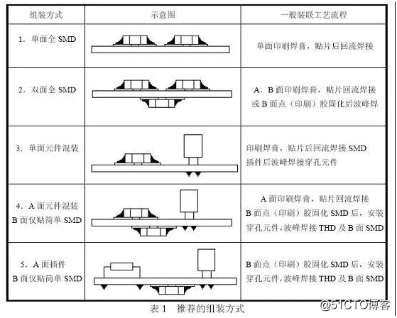
typically a PCB mounted with different density, as recommended by assembling a square circuit design engineer, should be installed on the PCB design linking step process to have a correct understanding, so you can avoid making some of the mistakes of principle. In the choice of assembly methods, in addition to considering the density of the PCB assembly, the ease of wiring, but also must be assembled according to an exemplary embodiment of this process, taking into account the level of process equipment enterprise itself. If the enterprise is no better €€ wave soldering process, then the fifth assembly methods on the selection list may put them at a lot of trouble.
Also worth noting is that if the program welded surface wave soldering process embodiment, the welding surface is arranged to be avoided SMD few have caused process complicated.
Component layout
On the PCB component layout have a very important impact on production efficiency and cost, it is a measure of PCB design can be fitted with an important indicator of. Generally, the components uniformly, regularly, aligned as far as possible, according to the same direction, the polarity distribution arrangement. A regular arrangement facilitates inspection, help to improve the placement / velocity plug, uniformly distributed and help to optimize the heat welding process.
On the other hand, it is a simplified process flow, PCB designers have always been clear, in any side of PCB, but to use reflow soldering process, and one group in wave soldering. This point is a large packing density, PCB welding surfaces must be more distribution when chip components, is particularly noteworthy. To consider what the designer group of welding process using welding surface mount components, most preferably using wave soldering process after curing the patch, the device can be simultaneously perforating pin element welding face; but peaks SMD components soldered relatively strict constraints, only 0603 and larger welding chip RC, SOT, SOIC (≥1mm lead pitch and a height less than 2.0mm).
Distributed components welding surface, when the PCB conveying direction perpendicular Fang Xiangyi connected to a wave soldering pins, to ensure that both sides of the welding ends or leads simultaneously dip soldering components, arrangement order and spacing between adjacent elements should also satisfy wave soldering required to avoid "shadowing effect", as shown in FIG 1. When a wave soldering and other multi-pin SOIC element shall last two (one per each side) at the weld toe pads disposed theft tin, tin-flow direction, to prevent even welding.
02PCB must be arranged on the gripping edge for automated production, alignment marks, positioning holes technology
is currently one of the electronics assembly industry, the highest degree of automation, automation equipment used require automatic transfer PCB, this will require the PCB the transport direction (normally the longitudinal direction), each with a vertical width of not less than 3-5mm clamping edge, in order to facilitate automatic transfer, near the edge of the board to avoid since the components can not be automatically loaded clamping joint.
Positioning mark role is widely used for positioning the optical assembly equipment, it is necessary to provide at least two to three PCB positioning marks, the optical recognition system for accurate positioning of the PCB and the PCB error correction processing. Positioning mark generally used, there are two marks must be distributed on a diagonal line of the PCB. Positioning mark selection is generally used like a pad filled circle graphics standard, for ease of identification, there should be a marked around the circuit features no other marks or open area, preferably not less than the diameter size of markers from the edge of the board should be 5mm the above.
Rational use of puzzle 03, to improve production efficiency and flexibility
at the time of the small dimensions of the PCB or irregular shape fitted together, it will be subject to many restrictions, so the puzzle typically uses several ways to make small PCB spliced into a suitable the size of the PCB mounted with, as shown in FIG 5. Usually the PCB unilateral size of less than 150mm, are considered puzzle embodiment, fight through two, three fight, fight other four, the large size of the PCB to fight suitable processing range and is generally wide 150mm ~ 250mm, length 250mm ~ 350mm the automated PCB loading-linking suitable size.
PCB manufacturability issues which need to be considered when designing?
Guess you like
Origin blog.51cto.com/14507444/2464176
Recommended
Ranking