Table of contents
3. Design and configuration of IP core
4. Experimental results and analysis
2. Simulation waveform and analysis
(1) Introduction to some indicators of the waveform
(2) Verification of the waveform conversion function
3. Download test results and analysis
1. Purpose of the experiment
(1) Master the principle of the signal generator;
(2) Learning complex digital system design;
(3) Learning to design with IP cores;
(4) Learn to use an online logic analyzer to observe the signals generated by the FPGA.
2. Design requirements
(1) The digitized waveform data is stored in ROM, and ROM is designed with IP core;
(2) Sine wave, square wave, and sawtooth wave are optional, and the digital tube displays the selected waveform type;
(3) The signal frequency and amplitude are adjustable and the frequency and amplitude are displayed by digital tubes;
(4) Connect the development board, and observe the amplitude and frequency modulation waveform of the signal online;
(5) DDS principle can be used to generate sinusoidal signal.
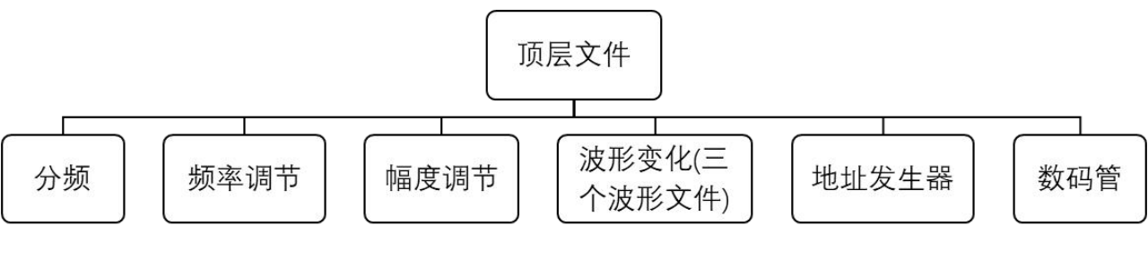
3. Experiment code
Due to space limitations, only the top-level file code is given here
-
module TOP(
input clk,
input rst_n,
input [1:0] wave,
//input [11:0]  p_word,
input [2:0]  AM,
input [3:0]    f_set,
//output [11:0] dac_dataa,
output[10:0] count_display//数码管输出
);
wire [31:0] f_word;
wire [4:0] amplitude;
wire [11:0] dac_dataa;
wire [1:0] cnt_1;
wire [6:0] cnt_2;
wire [2:0] cnt_3;
wire [31:0] fre;
 //   分频:
reg[26:0] clk_cnt;
reg  [2:0]  sel=4'b0;
reg clk1;
//reg  [10:0] count_display=11'b1111_1111111;
always @(posedge clk)
    begin
        clk_cnt=clk_cnt+1;
        if(clk_cnt==100000000)
            begin
            clk_cnt=0;
            clk1=1'b1;
            end
        else
            clk1=1'b0;

        if(clk_cnt%100000==0)
            begin
            sel=sel+1;
            if(sel==4)
                sel=0;
            end
    end
DDS uut1(
.clk(clk),
.rst_n(rst_n),
.wave(wave),
.f_word(f_word),
//.p_word(p_word),
.amplitude(amplitude),
.dac_dataa(dac_dataa),
.cnt_1(cnt_1)
);
F_word_set uut2(
.clk(clk),
.rst_n(rst_n),
.f_set(f_set),
.f_word(f_word),
.fre(fre),
.cnt_2(cnt_2)
);
A_set uut3(
.clk(clk),
.rst_n(rst_n),
.AM(AM),
.amplitude(amplitude),
.cnt_3(cnt_3)
);
display SG_display(
    .clk (clk),
    .rst (rst_n),
    .counter_1 (cnt_1),
    .counter_2 (cnt_2),
    .counter_3 (cnt_3),
    .count_display (count_display),
    .sel(sel)
);

ila_0 ila (
 .clk(clk), // input wire clk
 .probe0(dac_dataa), // input wire [11:0]  probe0
 .probe1(wave), // input wire [1:0]  probe1
 .probe2(AM), // input wire [2:0]  probe2
 .probe3(f_set) // input wire [3:0]  probe3
);
endmodule
1. Code principle analysis
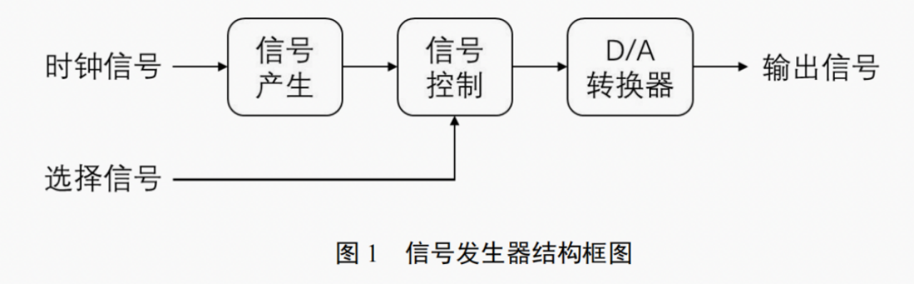
The sinusoidal signal generator consists of a counter or address generator (6 bits), sinusoidal signal data ROM ( 6-bit address lines, 8-bit data lines, containing 64 8-bit data, one cycle), schematic top-level design and 8-bit D/ a. Its block diagram is shown in Figure 1. Among them, the signal generation module will generate various signals required. There are many ways to generate these signals, such as using a counter to directly generate signal output, or using a counter to generate memory addresses, and store signal output data in the memory. The control module of the signal generator can be realized with a data selector. The waveform data is sent to the D/A converter, and the digital signal is converted into an analog signal for output.
2. Code Design Ideas
3. Design and configuration of IP core
(Take ila_0 as an example)
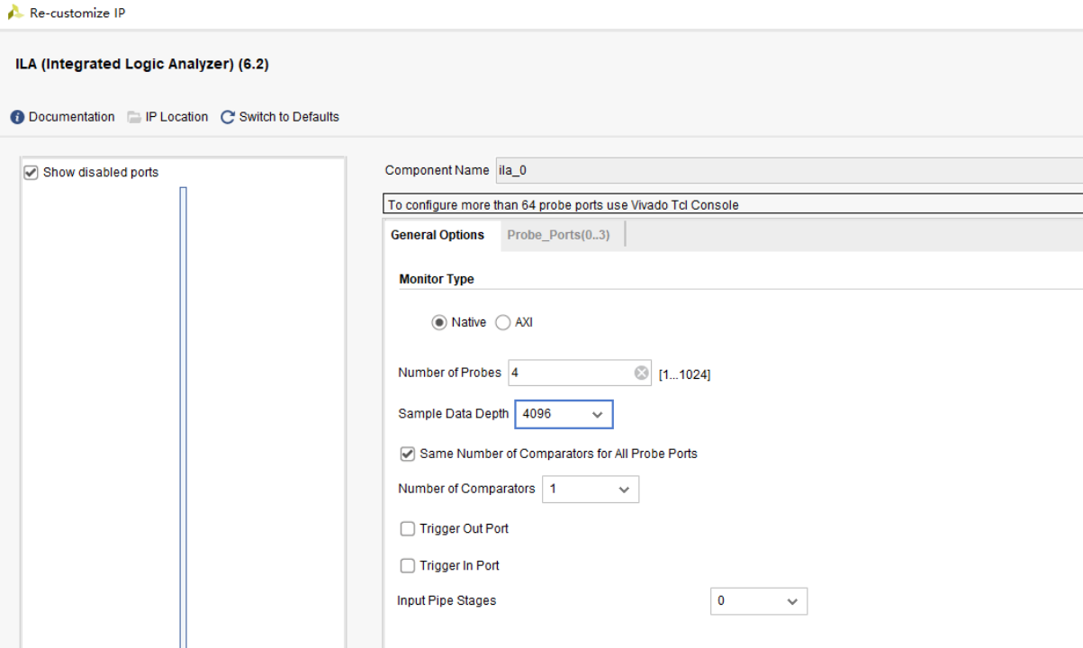
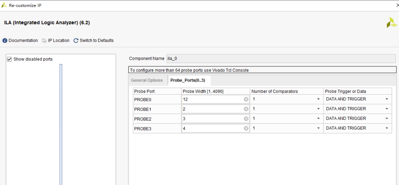
Configuration of Inline Logic Analyzer
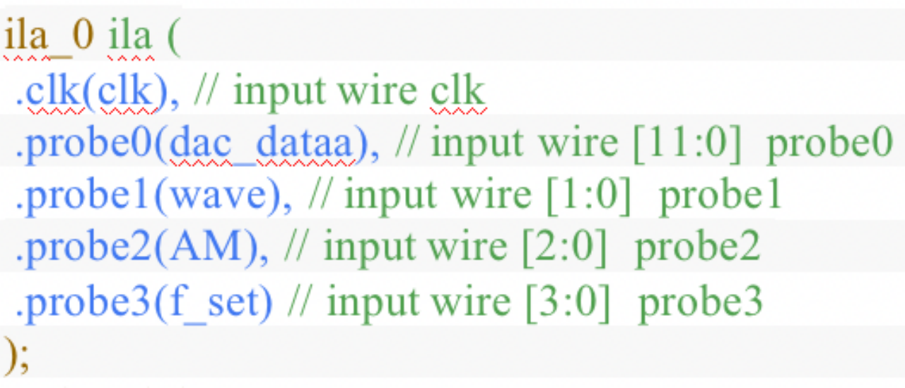
5 probes are set up here, and the changes in frequency, amplitude, and waveform type are displayed in the logic analyzer.
4. Experimental results and analysis
1. Pin lock
set_property -dict { PACKAGE_PIN W5 IOSTANDARD LVCMOS33 } [get_ports clk]
create_clock -add -name sys_clk_pin -period 10.00 -waveform {0 5} [get_ports clk]
## Switches
set_property -dict { PACKAGE_PIN V17 IOSTANDARD LVCMOS33 } [get_ports {wave[0]}]
set_property -dict { PACKAGE_PIN V16 IOSTANDARD LVCMOS33 } [get_ports {wave[1]}]
set_property -dict { PACKAGE_PIN W16 IOSTANDARD LVCMOS33 } [get_ports {f_set[0]}]
set_property -dict { PACKAGE_PIN W17 IOSTANDARD LVCMOS33 } [get_ports {f_set[1]}]
set_property -dict { PACKAGE_PIN W15 IOSTANDARD LVCMOS33 } [get_ports {f_set[2]}]
set_property -dict { PACKAGE_PIN V15 IOSTANDARD LVCMOS33 } [get_ports {f_set[3]}]
set_property -dict { PACKAGE_PIN W14 IOSTANDARD LVCMOS33 } [get_ports {AM[0]}]
set_property -dict { PACKAGE_PIN W13 IOSTANDARD LVCMOS33 } [get_ports {AM[1]}]
set_property -dict { PACKAGE_PIN V2 IOSTANDARD LVCMOS33 } [get_ports {AM[2]}]
set_property -dict { PACKAGE_PIN R2 IOSTANDARD LVCMOS33 } [get_ports {rst_n}]
##7 Segment Display
set_property -dict { PACKAGE_PIN W7 IOSTANDARD LVCMOS33 } [get_ports {count_display[6]}]
set_property -dict { PACKAGE_PIN W6 IOSTANDARD LVCMOS33 } [get_ports {count_display[5]}]
set_property -dict { PACKAGE_PIN U8 IOSTANDARD LVCMOS33 } [get_ports {count_display[4]}]
set_property -dict { PACKAGE_PIN V8 IOSTANDARD LVCMOS33 } [get_ports {count_display[3]}]
set_property -dict { PACKAGE_PIN U5 IOSTANDARD LVCMOS33 } [get_ports {count_display[2]}]
set_property -dict { PACKAGE_PIN V5 IOSTANDARD LVCMOS33 } [get_ports {count_display[1]}]
set_property -dict { PACKAGE_PIN U7 IOSTANDARD LVCMOS33 } [get_ports {count_display[0]}]
#set_property -dict { PACKAGE_PIN V7 IOSTANDARD LVCMOS33 } [get_ports dp]
set_property -dict { PACKAGE_PIN U2 IOSTANDARD LVCMOS33 } [get_ports {count_display[7]}]
set_property -dict { PACKAGE_PIN U4 IOSTANDARD LVCMOS33 } [get_ports {count_display[8]}]
set_property -dict { PACKAGE_PIN V4 IOSTANDARD LVCMOS33 } [get_ports {count_display[9]}]
set_property -dict { PACKAGE_PIN W4 IOSTANDARD LVCMOS33 } [get_ports {count_display[10]}]
2. Simulation waveform and analysis
(1) Introduction to some indicators of the waveform
rst_n: Indicates the enable terminal clk: Indicates the clock cycle wave: Waveform type 0-sine wave 1-rectangular wave 2-triangular wave 3-sawtooth wave
AM: waveform amplitude f_set: waveform frequency
(2) Verification of the waveform conversion function
I: Change of waveform type: from sine wave to rectangular wave II: Change from rectangular wave to sawtooth wave

III: Change from sawtooth to triangle
(3) Verification of the amplitude adjustment function --- the change of the amplitude of the triangle wave
(4) Verification of the frequency modulation function --- take the change of the frequency of the triangle wave as an example
analyze:
When the type, frequency, and amplitude of the signal change, the specific waveform will immediately change significantly, realizing the adjustability of frequency, amplitude, and waveform type.
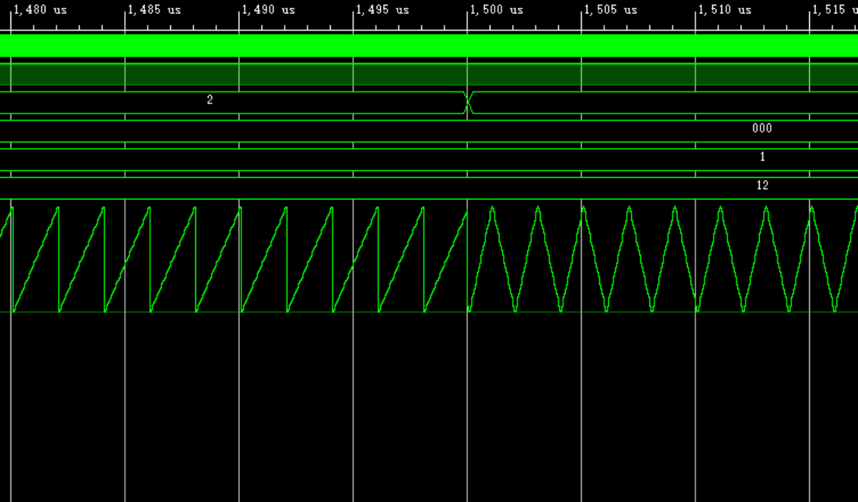
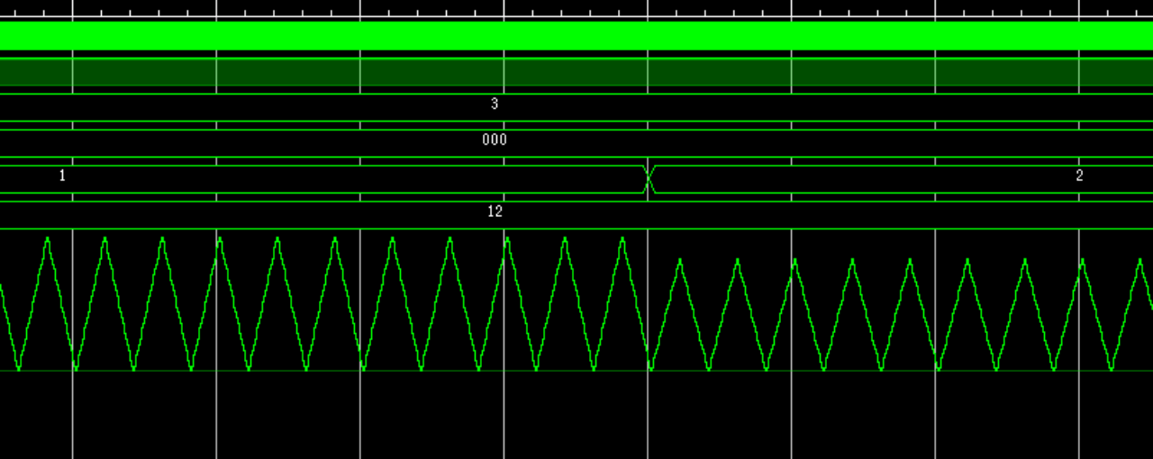
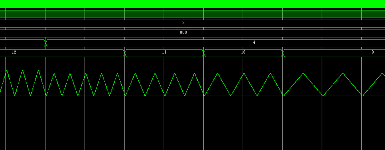
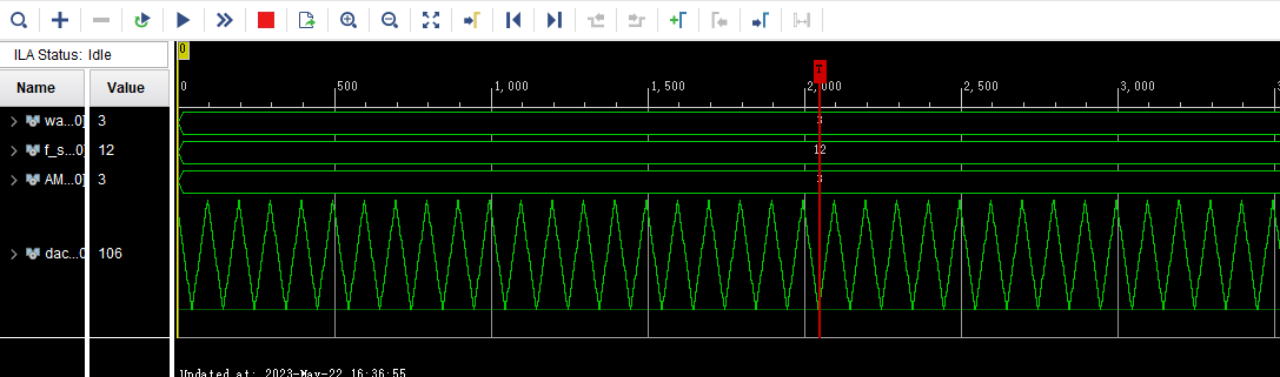
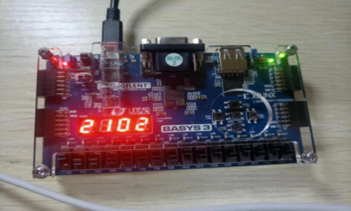
3. Download test results and analysis
Including online logic analyzer and development board
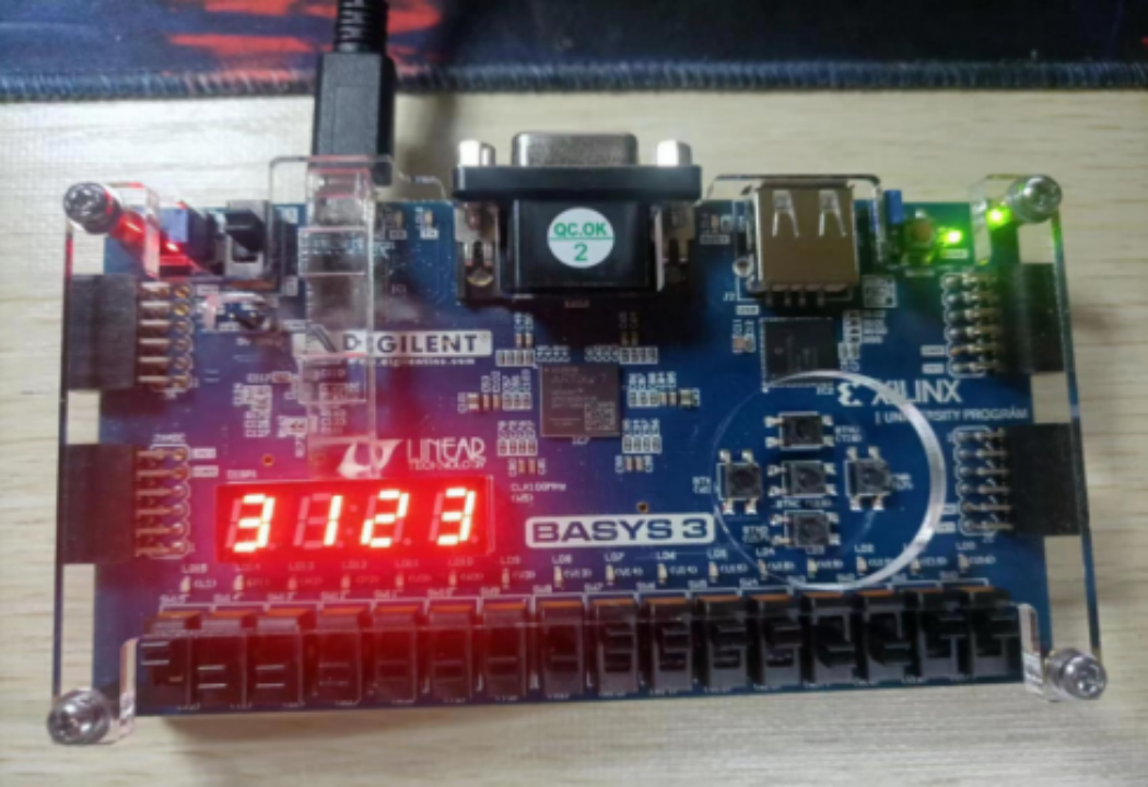
Waveform type: 0-sine wave 1-rectangular wave 2-triangular wave 3-sawtooth wave
Constantly changing waveform type, amplitude and frequency
- sawtooth wave
Amplitude: 3 Frequency: 12 Waveform Type: 3 Development Board
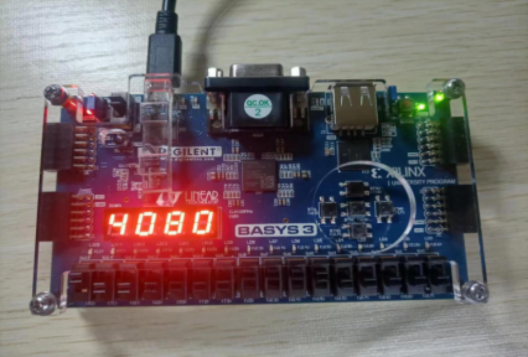
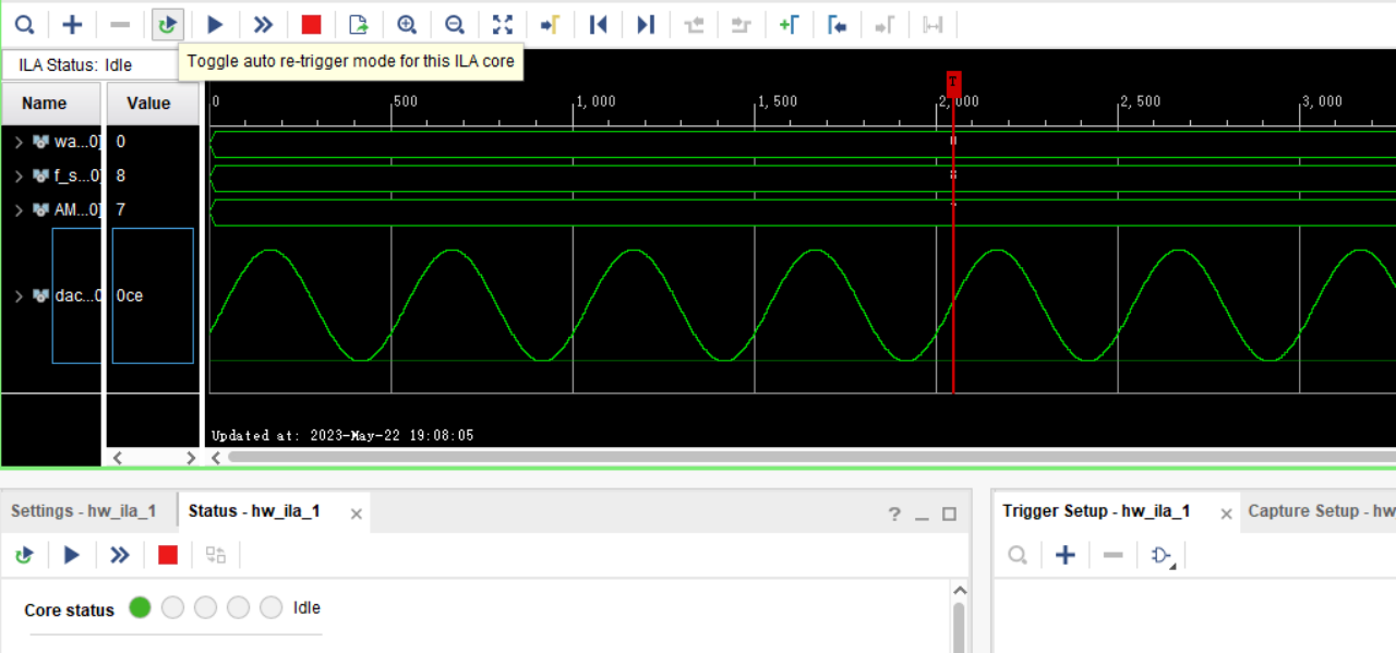
(2) Sine wave
Amplitude: 4 Frequency: 8 Waveform Type: 0 Development Board
(3) Rectangular wave
Amplitude: 1 Frequency: 7 Waveform Type: 1 Development Board

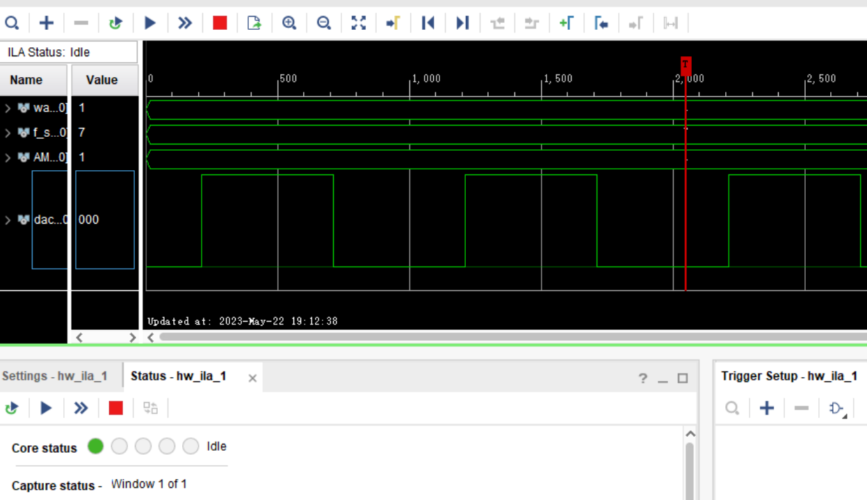
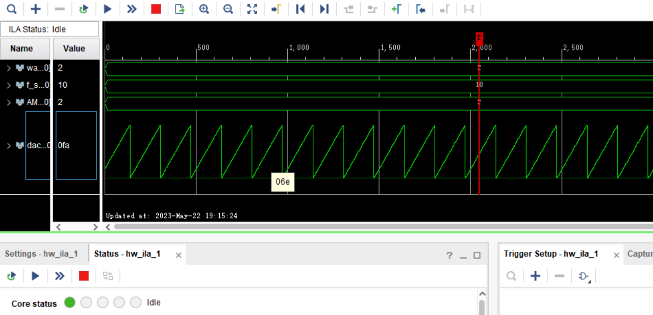
(4) Triangular wave
Amplitude: 2 Frequency: 10 Waveform Type: 2 Development Board
5. Experimental experience
1. During the experiment, after the simulation experiment was completed, the development board was prepared for testing, but it was found that this experiment was a little different from the previous experiment on the board. After consulting the relevant information, I realized that this physical experiment can not only rely on the bassy3 development board, but also needs to use an online logic analyzer to observe the signal generated by the FPGA, realize the display of the waveform, and show its frequency, amplitude and waveform type. Physical experiments have a different understanding.
2. At the beginning of the experiment, I was really at a loss. Although the experiment requires IP core design , although there is a certain idea, it is not clear how to start. Finally, I refer to the methods and procedures on the Internet to understand it a little bit. Of course, there are many discrepancies between the content on the Internet and our experiments, so we still need to make many modifications after understanding. For steps such as " the digitized waveform data is stored in the ROM, and the ROM is designed with an IP core" , if I did not refer to online tutorials, I would have to spend a lot of time digesting and understanding . Knowledge that can be digested and absorbed and transformed into oneself can also be understood . After this experiment, I really gained a lot, such as understanding the design principle of the signal generator , and learning to use the DDS principle to generate sinusoidal signals . Especially the understanding of ip core design , which also provides me with more choices for verilog programming in the future , and can also provide a lot of help for my subsequent experiments.
2022-05-05