Table of contents
2. Part of the code of the simulation file
3. System engineering documents
4. Experimental results and analysis
2. Simulation waveform and analysis
3. Download test results and analysis
1. Purpose of the experiment
(1) Master the communication signal modulation process and realization principle;
(2) Understand the optimization scheme in the design;
(3) Further study the design of complex digital systems;
(4) Cultivate engineering thinking and innovative thinking.
2. Design requirements
(1) To implement a single-channel PWM signal module, the initial phase, frequency, and duty cycle can be set through the port;
(2) Through the module call method, realize three-way PWM signal output, distinguish and display the phase, frequency, and duty cycle are adjustable;
(3) Add sine waveform VTH(t) to realize SPWM waveform;
3. Experiment code
1. Top-level file code
Due to space limitations, only the top-level code is given here
-
`timescale 1ns / 1ps

module PWM1(
                    input        clk,               //systerm clock  50MHz
     input       rst_n,
     input        fclock,//频率设置信号
     input        xclock ,//相位设置信号
     input        zclock,//占空比设置信号
        input[1:0]f,
        input[1:0]x,
        input[1:0]z,
     output    pwm1,
     output    pwm2,
     output    pwm3,
     output    pwm4,

     //output    [7:0]CNT2,
     //output    [7:0]CNT2,
     //output    [7:0]CNT3,
     //output    [7:0]CNT4
     output    [9:0]dataout
    );

wire [7:0]CNT1;
wire[7:0]CNT2;
wire [7:0]CNT3;
wire [7:0]CNT4;
//wire [9:0]dataout;
reg [19:0]count=0;
reg [30:0]count2=0;
reg [2:0] sel=0;
parameter T1MS=50000;


//仿真
//wire clk1;
//assign clk1=clk;
//板子
reg clk1;
always @(posedge clk)
 begin count2=count2+1;
  if(count2/100000%2==1) begin clk1=1'b1; count2=0;end
  else clk1=1'b0;
 end
//频率变换
pwm_gen U1(.clk(clk),.rst_n(rst_n),.fclock(fclock),.xclock(0),.zclock(0),.f(f),.x(x),.z(z),.pwm(pwm1),.CNT(CNT1));
//相位变换
pwm_gen U2(.clk(clk),.rst_n(rst_n),.fclock(0),.xclock(xclock),.zclock(0),.f(f),.x(x),.z(z),.pwm(pwm2),.CNT(CNT2));
//占空比变换
pwmz U3(.clk(clk),.rst_n(rst_n),.fclock(0),.xclock(0),.zclock(zclock),.f(f),.x(x),.z(z),.pwm(pwm3),.CNT(CNT3));

//SPWM
SPWM U4(.clk(clk),.rst_n(rst_n),.fclock(0),.xclock(0),.zclock(0),.f(0),.z(0),.x(0),.pwm(pwm4),.CNT(CNT4),.dataout(dataout));

ila_0 U5 (
 .clk(clk), // input wire clk


 .probe0(pwm1), // input wire [0:0]  probe0
 .probe1(pwm2), // input wire [0:0]  probe1
 .probe2(pwm3), // input wire [0:0]  probe2
 .probe3(pwm4), // input wire [0:0]  probe3
 .probe4(dataout)
);

endmodule
2. Part of the code of the simulation file
module gen_PWMTB(
    );
reg clk;
reg rst_n;
reg fclock;
reg xclock;
reg zclock;
reg [1:0]f;
reg [1:0]x;
reg [1:0]z;
wire pwm1;
wire pwm2;
wire pwm3;
wire pwm4;
//wire [7:0] CNT1;
//wire [7:0] CNT2;
//wire [7:0] CNT3;
wire [7:0] CNT4;
wire [9:0]dataout;

initial begin
rst_n=0;
clk=0;
fclock=0;
xclock=0;
zclock=0;
f<=2'd0;
x<=2'd0;
z<=2'd0;
#2;
rst_n=1;
#2200;
fclock<=1;
f<=2'd1;
xclock<=1;
x<=2'd1;
zclock<=1;
z<=2'd1;
#
end
always #10 clk=~clk;
PWM1 U0(clk,rst_n,fclock,xclock,zclock,f,x,z,pwm1,pwm2,pwm3,pwm4,CNT4,dataout);
endmodule
3. System engineering documents
4. Experimental results and analysis
1. Pin lock
set_property CLOCK_DEDICATED_ROUTE FALSE [get_nets fclock]
set_property CLOCK_DEDICATED_ROUTE FALSE [get_nets xclock]
set_property CLOCK_DEDICATED_ROUTE FALSE [get_nets zclock]
set_property PACKAGE_PIN W5 [get_ports clk]
set_property PACKAGE_PIN U16 [get_ports {dataout[0]}]
set_property PACKAGE_PIN E19 [get_ports {dataout[1]}]
set_property PACKAGE_PIN U19 [get_ports {dataout[2]}]
set_property PACKAGE_PIN V19 [get_ports {dataout[3]}]
set_property PACKAGE_PIN W18 [get_ports {dataout[4]}]
set_property PACKAGE_PIN U15 [get_ports {dataout[5]}]
set_property PACKAGE_PIN U14 [get_ports {dataout[6]}]
set_property PACKAGE_PIN V14 [get_ports {dataout[7]}]
set_property PACKAGE_PIN V13 [get_ports {dataout[8]}]
set_property PACKAGE_PIN V3 [get_ports {dataout[9]}]
set_property PACKAGE_PIN V17 [get_ports {f[0]}]
set_property PACKAGE_PIN V16 [get_ports {f[1]}]
set_property PACKAGE_PIN W16 [get_ports fclock]
set_property PACKAGE_PIN L1 [get_ports pwm1]
set_property PACKAGE_PIN P1 [get_ports pwm2]
set_property PACKAGE_PIN N3 [get_ports pwm3]
set_property PACKAGE_PIN P3 [get_ports pwm4]
set_property PACKAGE_PIN R2 [get_ports rst_n]
set_property PACKAGE_PIN W17 [get_ports {x[0]}]
set_property PACKAGE_PIN W15 [get_ports {x[1]}]
set_property PACKAGE_PIN V15 [get_ports xclock]
set_property PACKAGE_PIN W14 [get_ports {z[0]}]
set_property PACKAGE_PIN W13 [get_ports {z[1]}]
set_property PACKAGE_PIN V2 [get_ports zclock]
2. Simulation waveform and analysis
The waveform is as follows
Pwm1 indicates the frequency of the pwm signal
Pwm1 indicates the phase of the pwm signal
Pwm3 represents the duty cycle of the pwm signal
(1) It can be observed that when the signal frequency is constant, the individual change of the phase and the corresponding change of the duty cycle

(2) It can be observed that in the case of constant signal phase, the separate change of frequency and the corresponding change of duty cycle

(3) SPWM function verification
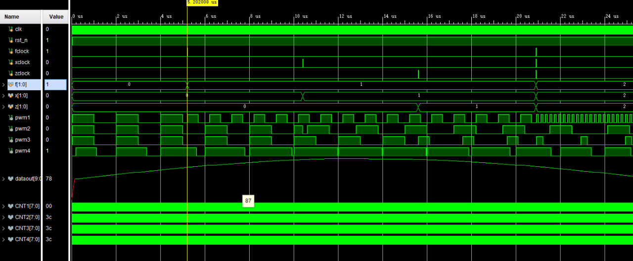
As shown in the figure, a complete cycle is realized, and the duty cycle of the output waveform changes with the sin waveform.
3. Download test results and analysis
The development board is as follows:

When the enable terminal is valid, after observing the signal input generated by the FPGA with an online logic analyzer, the waveform can be observed


Two waveforms with different ratios can show the adjustable signal frequency, phase and duty cycle.
5. Experimental experience
This experiment is really difficult and a headache, but fortunately, the acceptance is finally completed. Because although the previous experiments were divided into modules, they can actually run the simulation in one file. In this experiment, I also subconsciously wanted to compile the program in one file, but it was very difficult to implement, because there are different paths. Different points need to be taken care of. Moreover, the experiment requirement is to implement a multi-channel PWM signal generator through the module call method, so my writing method must be wrong, which also means that I have to learn new content, such as how to call the content of other files, how to update Design the top-level document well. But it's still a little bit off. In fact, the teacher's requirements are more detailed and more as the course progresses, which also shows that more attention should be paid to details in the design. At the beginning of this experiment, it was a little difficult for me to straighten out the requirements of the experiment. By the end of the experiment acceptance, I was able to tell how to write, how to operate, and the connection and application between various files. I feel my progress. I hope that I can learn more and make greater progress in the design and promotion of the big assignment ! I also hope that the design of this PWM signal modulator can lay a solid foundation for the comprehensive design !
2023-05-25