Transfer from: https://blog.csdn.net/gslscyx/article/details/103016237
Note: In this article, we briefly introduce the physical constraints of Xilinx FPGA pins, including location (pin) constraints and electrical constraints
1. Ordinary I/O constraints
Pin position constraints: set_property PAKAGE_PIN "pin number" [get_ports "port name"]
Pin level constraints: set_property IOSTANDARD "voltage" [get_ports "port name"]
Example:
set_property IOSTANDARD LVCMOS33 [get_ports sys_clk]
set_property IOST [ANDARD LVCMOS33] get_ports {led[0]}]
set_property IOSTANDARD LVCMOS33 [get_ports {led[1]}]
set_property PACKAGE_PIN U18 [get_ports sys_clk]
set_property PACKAGE_PIN M14 [get_ports {led[0]}]
set_property PACKAGE_PIN M15 [get_ports] ]
Note:
- 1) The above grammar is case sensitive;
- 2) When the port name is an array, it needs to be enclosed in {}, and the port name cannot be a keyword.
2. Differential signal constraints
2.1 Ordinary difference constraints
The differential signal constraint syntax is the same as in section 1. This is just an example.
1) HR I/O Bank, VCCO = 3.3V, HDMI interface constraints
set_property PACKAGE_PIN N18 [get_ports TMDS_clk_p]
set_property PACKAGE_PIN V20 [get_ports {TMDS_data_p[0]}]
set_property I [OSTANDARD TMDS_OST_33 [get_property I [OSTANDARD TMDS_OST]
TMDS_get_p TMDS_set_ 0]}]
2) HP I/O Bank, VCCO = 1.8V, HDMI interface constraints
set_property PACKAGE_PIN N18 [get_ports TMDS_clk_p]
set_property PACKAGE_PIN V20 [get_ports {TMDS_data_p[0]}]
set_property IOSTANDARD LVDS [get_property IOSTANDARD
IOST_get_ports get_ports {TMDS_data_p[0]}]
Note:
- 1) Differential signal constraint, only P pin is required, and the system automatically matches the N pin constraint. Of course, there is no problem with _P and _N pin constraints;
- 2) The level of the differential signal should be restricted according to the VCCO Bank voltage.
2.2 Transceiver differential signal constraints
1) Transceiver MGTREFCLK clock constraint
pin location constraint: set_property LOC "pin number" [get_ports "port name"]
Example:
set_property LOC G7 [get_ports Q2_CLK0_GTREFCLK_PAD_N_IN]
set_property LOC G8 [get_ports Q2_CLK0_GT_PMGIN_PAD
channel
for transceiver constraints 2) GTXE2_CHANNEL channel constraints: One method is to use the 7 series FPGAs transceiver wizard to automatically generate the XDC template after configuring the transceiver configuration parameters, and then apply the template to your own design; the second method is to write XDC yourself Constraint file, its position constraint position should refer to the specific schematic signal pin to write the constraint file.
Example: For the four-channel transceiver in Figure 1, the GTXE2_CHANNEL constraint.
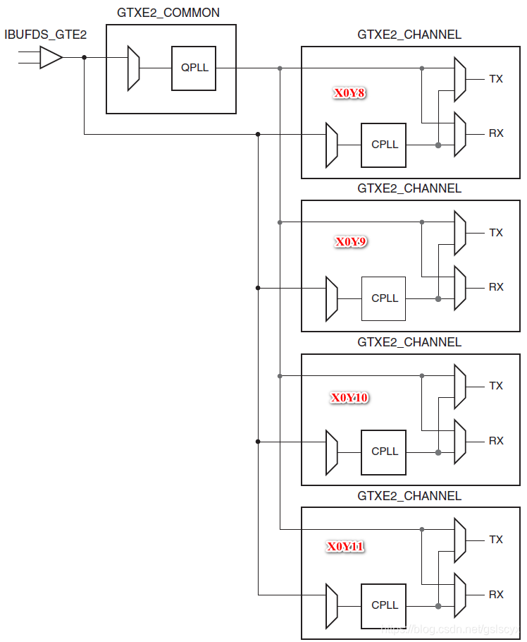
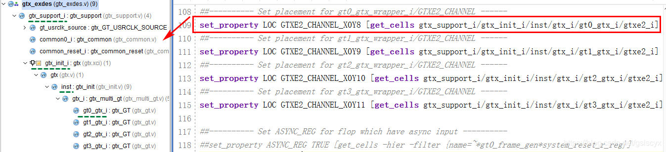
Transceiver channel position constraint: set_property LOC “GTXE2_CHANNEL_X* Y *” [get_cells “gtxe_2 instantiation path”]
##---------- Set placement for gt0_gtx_wrapper_i/GTXE2_CHANNEL ------
set_property LOC GTXE2_CHANNEL_X0Y8 [get_cells gtx_support_i/gtx_init_i/inst/gtx_i/gt0_gtx_i/gtxe2_i]
##---------- Set placement for gt1_gtx_wrapper_i/GTXE2_CHANNEL ------
set_property LOC GTXE2_CHANNEL_X0Y9 [get_cells gtx_support_i/gtx_init_i/inst/gtx_i/gt1_gtx_i/gtxe2_i]
##---------- Set placement for gt2_gtx_wrapper_i/GTXE2_CHANNEL ------
set_property LOC GTXE2_CHANNEL_X0Y10 [get_cells gtx_support_i/gtx_init_i/inst/gtx_i/gt2_gtx_i/gtxe2_i]
##---------- Set placement for gt3_gtx_wrapper_i/GTXE2_CHANNEL ------
set_property LOC GTXE2_CHANNEL_X0Y11 [get_cells gtx_support_i/gtx_init_i/inst/gtx_i/gt3_gtx_i/gtxe2_i]
Note:
Refer to Figure 2 for the gtxe_2 instantiation path. The path name is modified according to the specific project implementation.
How to view the actual pin location of the GTHE transceiver
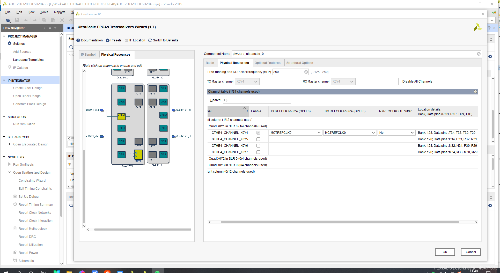
Search for the transceivers ip in the ip catalog to find the transceiver ip, which may have different names for different FPGA series.
Then you can view the pin location inside, and you can open the relevant documents to find information.
Xilinx IP core configuration, step by step verification of Xilinx Serdes GTX up to 8.0Gbps_kuangxin's blog -CSDN blog
https://blog.csdn.net/u010161493/article/details/77658599