We know that the memory does not have an address, to the memory allocation process called memory-mapped address, that what is mapped register? Register in the end is what?
Block2 in this area of the memory, on-chip peripherals are designed, they are four bytes as a unit, a total of 32bit, each cell corresponding to a different function, when we drive controlling these peripheral units may work. We can find the starting address of each unit and then to access these operating units by way of the C language pointer, if each time to access through this address, not just a bad memory but also prone to error, then we can Depending on the function of each unit to function in the name of the memory unit to take an alias, this alias is what we often say that the register, the memory unit has been allocated to a good address specific functional process is called alias register map .
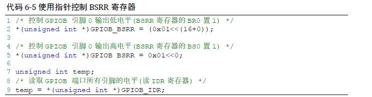
For example, we find the address output data register ODR GPIOB ports is 0x4001 0C0C (As to how to find this address can skip, we will explain in detail later), a register ODR 32bit, 16bit active low, corresponding to the outside 16 IO, 0/1 IO write is output corresponding to low / high. By the way we are now operating the C language pointer, so GPIOB of 16 IO will output high.
1 // GPIOB output ports are all high
2 *(unsigned int*)(0x4001 0C0C) = 0xFFFF;
0x4001 0C0C in our view GPIOB port ODR address, but the compiler view, this is just an ordinary variable, is an immediate, to get the compiler is also considered to be a pointer, we have to be cast, the it is converted into a pointer, i.e., (unsigned int *) 0x4001 0C0C, then this pointer operation *. We just say, bad memory access via absolute addresses memory unit and error-prone, we can operate through the register.
1 // GPIOB output ports are all high
2 #define GPIOB_ODR (unsigned int*)(GPIOB_BASE+0x0C)
3 * GPIOB_ODR = 0xFF;
For ease of operation, we just put a pointer operation "*" is also defined inside the alias register.
1 // GPIOB output ports are all high
2#define GPIOB_ODR * (unsigned int*)(GPIOB_BASE+0x0C)
3 GPIOB_ODR = 0xFF;
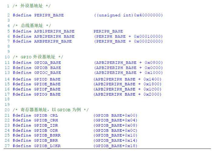
STM32 peripherals address mapping
On-chip peripheral bus is divided into three, depending on the peripheral speed different bus mount different peripherals, the APB1 mounted low-speed peripherals, and AHB mounted APB2 and high-speed peripherals. The base address of the corresponding address bus of the lowest we called the bus, the bus is also mounted on the base address of the first address bus peripherals. In which the peripheral bus address on APB1 lowest piece from here, also known as peripheral base address.
1. Bus base address
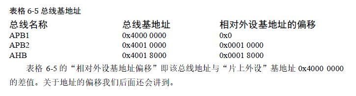
2. Peripheral base address
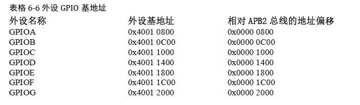
Bus hang carrying a variety of peripherals, these peripherals also have their own range of addresses, the first address of a specific peripheral called the "XX Peripheral base address", also known as peripheral boundary address XX. Section 2.3 relating to the specific peripheral boundary address STM32F10xx refer to "STM32F10xx Reference Manual" memory map Table 1: STM32F10xx boundary address register.
That which we GPIO to explain this to the base address of the peripheral peripheral, GPIO belongs to the high-speed peripherals, mount to the APB2 bus.
3. peripheral register
Within the address range of the peripheral XX, it is the distribution of the peripherals. In an example GPIO peripherals, is referred to as general-purpose GPIO input and output ports, is simply controlled STM32 pin, the basic function is to control the output pin high or low. The simplest application is the GPIO pins connected to the cathode of the LED, the anode of the LED lamp to the power, and by controlling the level of the STM32 pin, thus controlling the LED light off.
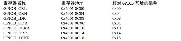
There are many GPIO registers, each with a specific function. Each register is 32bit, total of four bytes, arranged in order on the peripheral base address, the relative position of the register to all peripheral base address offset address will be described. Here we GPIOB port as an example to illustrate what are GPIO register.
Related peripherals Register Description Register Description section refer to specific sections of "STM32F10xx Reference Manual", in the program when we require repeated access to peripheral register descriptions.
Here we are with "GPIO port set / reset register" for example, tells you how to understand the explanation register.
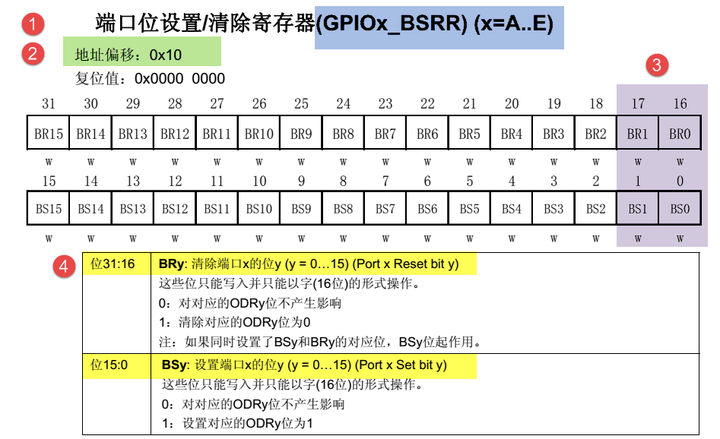
① Name
寄存器说明中首先列出了该寄存器中的名称,“(GPIOx_BSRR)(x=A…E)”这段的意思是该寄存器名为“GPIOx_BSRR”其中的“x”可以为A-E,也就是说这个寄存器说明适用于GPIOA、GPIOB 至GPIOE,这些GPIO端口都有这样的一个寄存器。
②偏移地址
偏移地址是指本寄存器相对于这个外设的基地址的偏移。本寄存器的偏移地址是0x18,从参考手册中我们可以查到GPIOA 外设的基地址为0x4001 0800 ,我们就可以算出GPIOA的这个GPIOA_BSRR 寄存器的地址为:0x4001 0800+0x18 ;同理,由于GPIOB 的外设基地址为0x4001 0C00,可算出GPIOB_BSRR 寄存器的地址为:0x4001 0C00+0x18 。其他GPIO端口以此类推即可。
③寄存器位表
紧接着的是本寄存器的位表,表中列出它的0-31 位的名称及权限。表上方的数字为位编号,中间为位名称,最下方为读写权限,其中w 表示只写,r 表示只读,rw 表示可读写。本寄存器中的位权限都是w,所以只能写,如果读本寄存器,是无法保证读取到它真正内容的。而有的寄存器位只读,一般是用于表示STM32 外设的某种工作状态的,由STM32硬件自动更改,程序通过读取那些寄存器位来判断外设的工作状态。
④位功能说明
位功能是寄存器说明中最重要的部分,它详细介绍了寄存器每一个位的功能。例如本寄存器中有两种寄存器位,分别为BRy 及BSy,其中的y 数值可以是0-15,这里的0-15表示端口的引脚号,如BR0、BS0 用于控制GPIOx 的第0 个引脚,若x 表示GPIOA,那就是控制GPIOA的第0 引脚,而BR1、BS1 就是控制GPIOA 第1 个引脚。
其中BRy 引脚的说明是“0:不会对相应的ODRx 位执行任何操作;1:对相应ODRx位进行复位”。这里的“复位”是将该位设置为0 的意思,而“置位”表示将该位设置为1;说明中的ODRx 是另一个寄存器的寄存器位,我们只需要知道ODRx 位为1 的时候,对应的引脚x 输出高电平,为0 的时候对应的引脚输出低电平即可(感兴趣的读者可以查询该寄存器GPIOx_ODR 的说明了解)。所以,如果对BR0 写入“1”的话,那么GPIOx 的第0 个引脚就会输出“低电平”,但是对BR0 写入“0”的话,却不会影响ODR0 位,所以引
脚电平不会改变。要想该引脚输出“高电平”,就需要对“BS0”位写入“1”,寄存器位BSy 与BRy 是相反的操作。
C 语言对寄存器的封装
1. 封装总线和外设基地址
在编程上为了方便理解和记忆,我们把总线基地址和外设基地址都以相应的宏定义起来,总线或者外设都以他们的名字作为宏名。
首先定义了 “片上外设”基地址PERIPH_BASE,接着在PERIPH_BASE 上加入各个总线的地址偏移, 得到APB1 、APB2 总线的地址APB1PERIPH_BASE 、APB2PERIPH_BASE,在其之上加入外设地址的偏移,得到GPIOA-G的外设地址,最后在外设地址上加入各寄存器的地址偏移,得到特定寄存器的地址。一旦有了具体地址,就可以用指针读写。
该代码使用 (unsigned int *) 把GPIOB_BSRR 宏的数值强制转换成了地址,然后再用“*”号做取指针操作,对该地址的赋值,从而实现了写寄存器的功能。同样,读寄存器也是用取指针操作,把寄存器中的数据取到变量里,从而获取STM32 外设的状态。
2. 封装寄存器列表
用上面的方法去定义地址,还是稍显繁琐,例如GPIOA-GPIOE 都各有一组功能相同的寄存器,如GPIOA_ODR/GPIOB_ODR/GPIOC_ODR 等等,它们只是地址不一样,但却要为每个寄存器都定义它的地址。为了更方便地访问寄存器,我们引入C 语言中的结构体语法对寄存器进行封装。
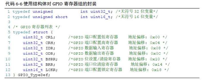
这段代码用typedef 关键字声明了名为GPIO_TypeDef 的结构体类型,结构体内有7 个成员变量,变量名正好对应寄存器的名字。C 语言的语法规定,结构体内变量的存储空间是连续的,其中32 位的变量占用4 个字节,16 位的变量占用2 个字节。
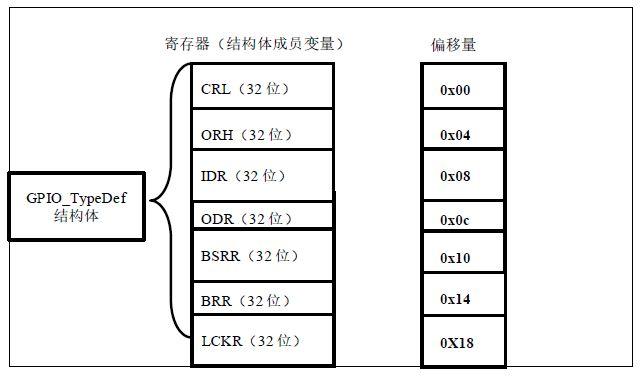
也就是说,我们定义的这个GPIO_TypeDef ,假如这个结构体的首地址为0x40010C00(这也是第一个成员变量CRL 的地址), 那么结构体中第二个成员变量CRH 的地址即为0x4001 0C00 +0x04 ,加上的这个0x04 ,正是代表CRL 所占用的4 个字节地址的偏移量,其它成员变量相对于结构体首地址的偏移,在上述代码右侧注释已给。
这样的地址偏移与STM32 GPIO 外设定义的寄存器地址偏移一一对应,只要给结构体设置好首地址,就能把结构体内成员的地址确定下来,然后就能以结构体的形式访问寄存器。
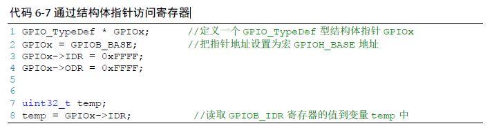
这段代码先用GPIO_TypeDef 类型定义一个结构体指针GPIOx,并让指针指向地址GPIOB_BASE(0x4001 0C00),使用地址确定下来,然后根据C 语言访问结构体的语法,用GPIOx->ODR 及GPIOx->IDR 等方式读写寄存器。
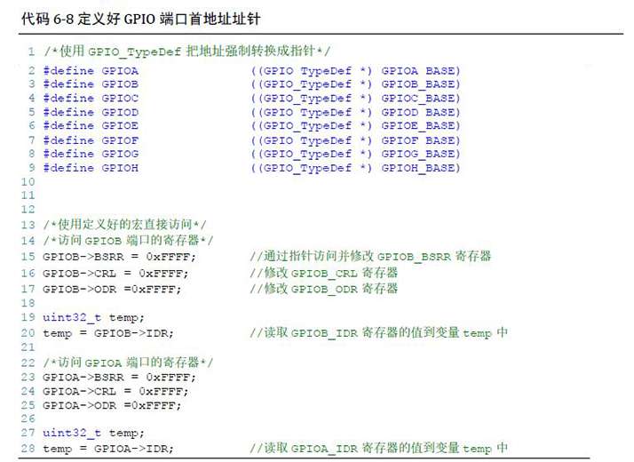
最后,我们更进一步,直接使用宏定义好GPIO_TypeDef 类型的指针,而且指针指向各个GPIO端口的首地址,使用时我们直接用该宏访问寄存器即可。
这里我们仅是以GPIO 这个外设为例,给大家讲解了C 语言对寄存器的封装。以此类推,其他外设也同样可以用这种方法来封装。好消息是,这部分工作都由固件库帮我们完成了,这里我们只是分析了下这个封装的过程,让大家知其然,也只其所以然。
stm32视频学习资料
STM32可以这样玩
http://www.makeru.com.cn/live/4034_1460.html?s=45051
分析STM32的的开发方式
http://www.makeru.com.cn/live/3523_1673.html?s=45051
释放潜能:学习效率提升、编程能力提升
http://www.makeru.com.cn/live/3507_1276.html?s=45051
从单片机到嵌入式linux我们需要做什么
http://www.makeru.com.cn/live/5413_1994.html?s=45051
stm32 如何用DMA搬运数据
http://www.makeru.com.cn/live/detail/1484.html?s=45051
(STM32中断系统)
http://www.makeru.com.cn/live/1392_1124.html?s=45051
pdf以及相关文档下载群:830802928