"STM32 Chinese Reference Manual V10" - Chapter 11 Analog/Digital Conversion (ADC)
Basic introduction to ADC
Basic Definition of ADC
Abbreviation for Analog-to-Digital Converter. Refers to an analog/digital converter or analog/digital converter. Refers to a device that converts an analog signal of a continuous variable into a discrete digital signal.
A typical analog-to-digital converter converts an analog signal into a digital signal representing a proportional voltage value.
Key Features of ADCs
- 12-bit successive approximation analog-to-digital converter;
- With up to 3 ADC controllers;
- Supports up to 23 channels and can measure up to 21 external and 2 internal signal sources;
- Support single and continuous conversion mode;
- End of conversion, end of injection conversion, and an interrupt when an analog watchdog event occurs;
- Auto scan mode from channel 0 to channel n;
- automatic calibration;
- The sampling interval can be programmed by channel;
- Both regular channels and injection channels have external trigger options;
- The conversion result supports left-aligned or right-aligned storage in the 16-bit data register;
- ADC conversion time: the maximum conversion rate is 1us (the maximum conversion rate is 1MHz, obtained when ADCCLK=14M, and the sampling period is 1.5 ADC clocks);
- ADC power supply requirements: 2.4V-3.6V;
- ADC input range: VREF- ≤ VIN ≤ VREF+.
STM32F10x series chip ADC channel and pin correspondence
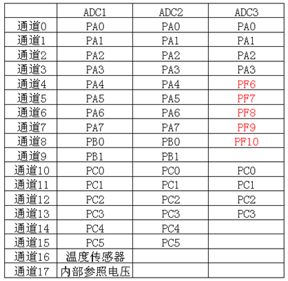
As can be seen from the above figure, STM32F103ZET6 with 3 ADC controllers supports a total of 23 channels, including 21 external and 2 internal signal sources; but each ADC controller can only have up to 18 channels, including 16 External and 2 internal signal sources.
Fundamentals of ADCs
Working block diagram of ADC
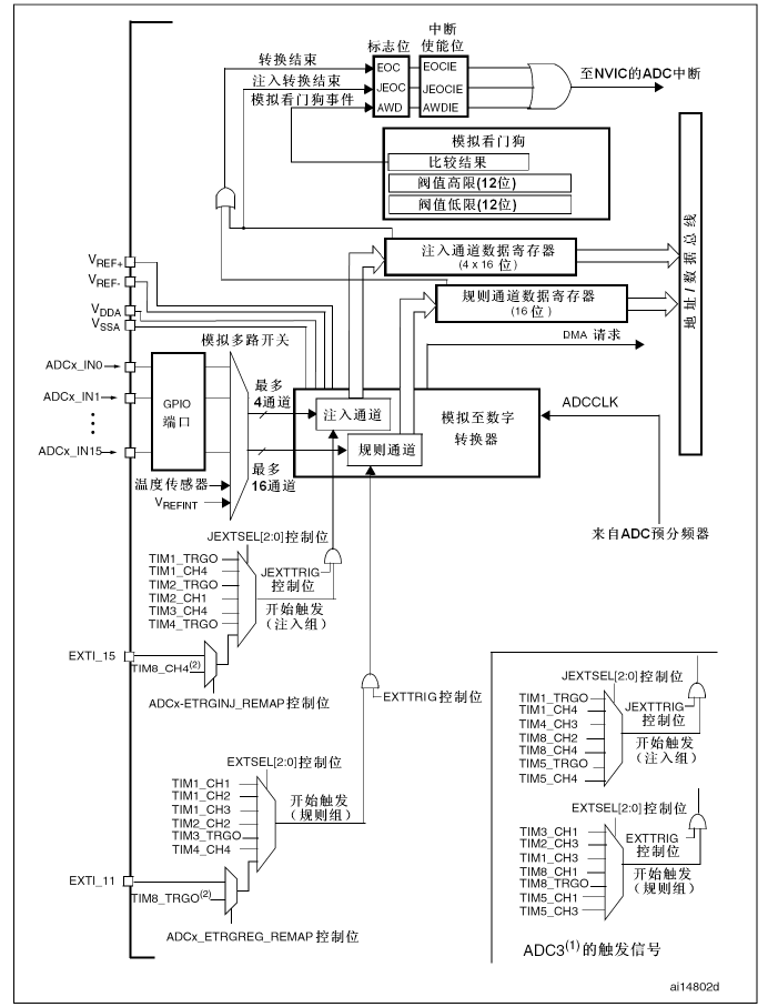
The block diagram of the ADC module looks complicated, and we will analyze it bit by bit.
ADC pin
The leftmost column in the block diagram is the various pins of the ADC. Their names, signal types and functions are shown in the following figure:
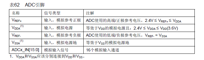
In general, VDD is 3.3V, VSS is grounded, correspondingly, VDDA is 3.3V, VSSA is also grounded, and the analog input signal should not exceed VDD (3.3V).
ADC Clock Configuration
The ADCCLK from the ADC prescaler noted in the block diagram is the clock source for the ADC module. Typically, the ADCCLK clock provided by the clock controller is synchronized with PCLK2 (APB2 clock). The RCC controller provides a dedicated programmable prescaler for the ADC clock.
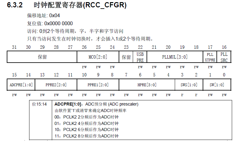
It is necessary to pay attention here, in general: do not let the ADC clock exceed 14MHz, otherwise it may be inaccurate.
That is to say, if PCLK2 is set to 72MHz by default, it should be divided by 6 or 8 at this time.
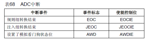
ADC interrupt
At the very top of the block diagram, the various interrupts for the ADC are shown. It is obvious to see that an interrupt can be generated at the end of a rule and injection group conversion, and an interrupt can also be generated when the analog watchdog status bit is set. They all have independent interrupt enable bits.
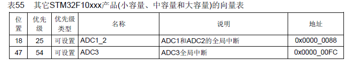
Note: The interrupts of ADC1 and ADC2 are mapped on the same interrupt vector, while the interrupt of ADC3 has its own interrupt vector.
There are three specific types of ADC interrupt events, as shown in the following figure:
ADC channel selection
I mentioned earlier that the end of ADC rule group conversion and the end of injection group conversion can generate interrupts, so what are rule groups and injection groups? This is the middle part of the block diagram.
The ADC controller of STM32 has many channels, so the module can switch to different input channels and convert through the internal analog multiplexer. STM32 has specially added a variety of group conversion modes, which can be automatically sampled and converted one by one for multiple analog channels after being set by the program. They can be organized into two groups: regular channel groups and injection channel groups.
For example, the conversion can be done in the following order: channel 3, channel 8, channel 2, channel 2, channel 0, channel 2, channel 2, channel 15.
- Regular channel group: Up to 16 channels can be arranged. The regular channel and its conversion order are selected in the ADC_SQRx register, and the total number of regular group conversions should be written into L[3:0] of the ADC_SQR1 register;
- Injection channel group: Up to 4 channels can be arranged. The injection group and its conversion order are selected in the ADC_JSQR register. The total number of conversions injected into the group should be written to L[1:0] of the ADC_JSQR register.
When performing regular channel group scan conversions, exceptions are made to enable conversions that inject channel groups.
Of course, there is a caveat: if the ADC_SQRx or ADC_JSQR registers are changed during a conversion, the current conversion is cleared and a new start pulse will be sent to the ADC to convert the newly selected bank.
Maybe it's just literal or not very understanding? We can understand more intuitively through graphics:

An inappropriate analogy is that the conversion of the regular channel group is like the normal execution of the program, and the conversion of the injection channel group is like an interrupt handler outside the normal execution of the program.
ADC conversion method
Each channel of the STM32 ADC can form a regular channel group or an injection channel group, but in the conversion mode, there can also be single conversion, continuous conversion, and scan conversion modes .
single conversion mode
In single conversion mode, the ADC performs only one conversion. This mode can be started either by setting the ADON bit of the ADC_CR2 register (applicable to regular channels only) or by external triggering (applicable to regular channels or injection channels), at which time the CONT bit is 0.
Continuous conversion mode
In continuous conversion mode, another conversion is started as soon as the previous ADC conversion is completed. This mode can be initiated by an external trigger or by setting the ADON bit on the ADC_CR2 register, where the CONT bit is 1.

scan mode
This mode is used to scan a group of analog channels.
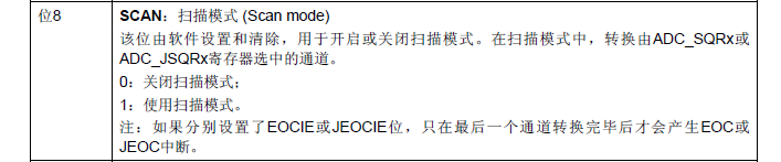
The scan mode can be selected by setting the SCAN bit in the ADC_CR1 register. Once this bit is set, the ADC scans all channels selected by the ADC_SQRX register (for regular channels) or ADC_JSQR (for injected channels). Perform a single conversion on each channel of each group. At the end of each conversion, the next channel of the same group is automatically converted. If the CONT bit is set, conversion does not stop on the last channel of the selection group, but resumes conversion from the first channel of the selection group again.
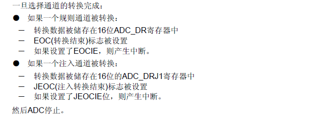
It should be noted here that if the interrupt is used in the scan mode, the interrupt will not be generated until the last channel is converted. For continuous conversion, an interrupt will be generated after each conversion.
If the DMA bit is set, after each EOC, the DMA controller transfers the conversion data of the regular set of channels to the SRAM. Instead, the converted data injected into the channel is always stored in the ADC_JDRx registers.
analog watchdog
In addition to the completion of regular group conversion and injection group conversion, the generation of ADC interrupts also includes analog watchdog events.
If the analog voltage converted by the ADC is below the low threshold or above the high threshold, the AWD analog watchdog status bit is set. The thresholds are located in the least significant 12 bits of the ADC_HTR and ADC_LTR registers. The corresponding interrupt is enabled by setting the AWDIE bit in the ADC_CR1 register.
Note that the threshold is independent of the data alignment mode selected by the ALIGN bits on the ADC_CR2 register. Comparison is done before alignment. That is, the comparison is done before the data is saved to the data register (data alignment is explained below)!
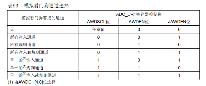
By configuring the ADC_CR1 register, the analog watchdog can act on one or more channels:
Externally Triggered Conversion
In the lower part of the block diagram, it is shown that regular transitions, injection transitions can be triggered by external events (eg timer capture, EXTI line) . External events can trigger conversions if the EXTTRIG control bit is set. The EXTSEL[2:0] and JEXTSEL2:0] control bits allow the application to select one of eight possible events that can trigger sampling of rules and injection groups.
Note: When the external trigger signal is selected as ADC rule or injection conversion, only its rising edge can start the conversion .
Automatic calibration
Calibrating the ADC has a built-in self-calibration mode. Calibration greatly reduces quasi-accuracy errors due to variations in the internal capacitor bank. During calibration, an error correction code (digital value) is calculated on each capacitor, and this code is used to remove errors that occur on each capacitor in subsequent conversions.
Calibration is initiated by setting the CAL bit in the ADC_CR2 register. Once calibration is complete, the CAL bit is reset by hardware and normal conversions can begin. It is recommended to perform an ADC calibration at power-up. After the calibration phase, the calibration code is stored in ADC_DR.
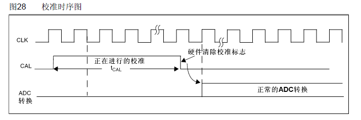
NOTE: It is recommended to perform a calibration after each power-up. The ADC must be powered off (ADON=0) for at least two ADC clock cycles before starting the calibration at the same time.
data alignment
Since the ADC of STM32 is a 12-bit successive approximation type analog-to-digital converter, the data is stored in a 16-bit register . Therefore, the ALIGN bit in the ADC_CR2 register selects the alignment of the converted data storage. Data can be left-aligned or right-aligned, as shown in the following image:
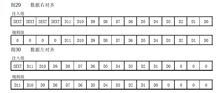
- The converted data value of the injected group channel has been subtracted by the offset defined in the ADC_JOFRx registers, so the result can be a negative value. The SEXT bit is the extended sign value.
- For regular group channels, the offset value does not need to be subtracted, so only 12 bits are valid.
Channel sampling time
The ADC samples the input voltage using several ADC_CLK cycles, the number of which can be changed by the SMP[2:0] bits in the ADC_SMPR1 and ADC_SMPR2 registers. Each channel can be sampled at a different time.
The total conversion time is calculated as follows:
TCONV = sample time + 12.5 cycles
For example: when ADCCLK=14MHz and the sampling time is 1.5 cycles, TCONV =1.5+12.5=14 cycles=1μs.
Therefore, the minimum sampling time of the ADC is 1us (the ADC clock is 14MHz, and the sampling period is 1.5 cycles) .
ADC related configuration registers
ADC Control Register 1 (ADC_CR1)
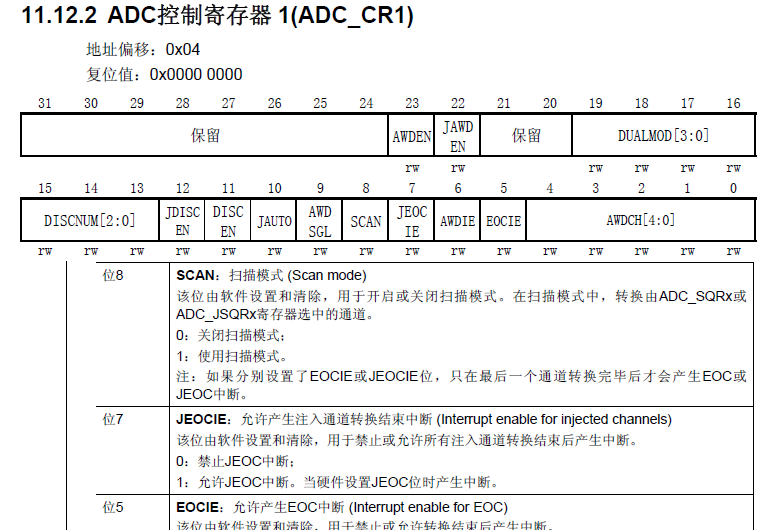
Function: set scan mode, interrupt enable (conversion end, injection conversion end, analog watchdog), dual mode selection (usually select independent mode), etc.
Note: In scan mode, the channel selected by the ADC_SQRx or ADC_JSQRx registers is converted. If EOCIE or JEOCIE is set, the EOC or JEOC interrupt will not be generated until the last channel is converted.
ADC Control Register 2 (ADC_CR2)
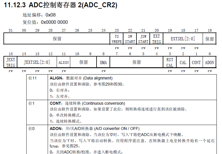
Function: Set data alignment, continuous conversion bit, ADC start bit, external trigger conversion (generally choose software conversion SWSTART, JSWSTART) .
ADC Sample Time Register x (ADC_SMPRx)
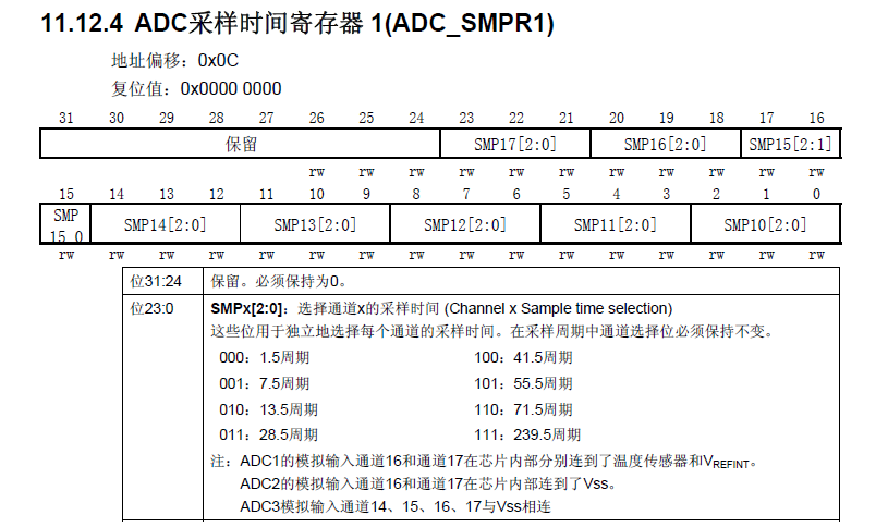
Function: Set the sampling time of each channel of ADC.
ADC Injection Channel Data Offset Register x (ADC_JOFRx)
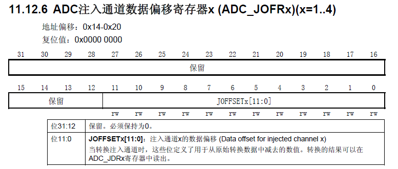
Function: Set the ADC injection channel data offset.
ADC Watchdog High/Low Threshold Register (ADC_HTR, ADC_LRT)
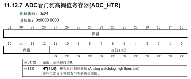
Function: Set the high and low thresholds of the ADC analog watchdog.
ADC Rules Sequence Register x (ADC_SQRx)
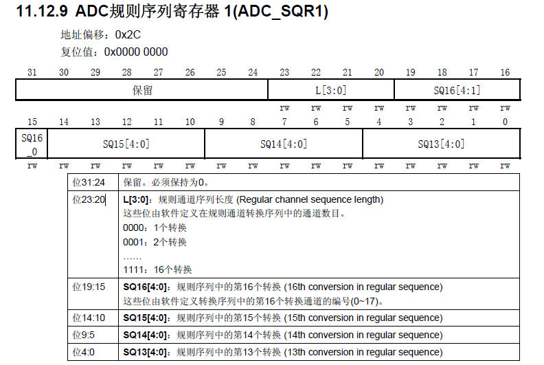
Function: Set the length of the regular channel sequence and the channel number corresponding to each conversion in the sequence (up to 16) .
ADC Injection Sequence Register (ADC_JSQR)
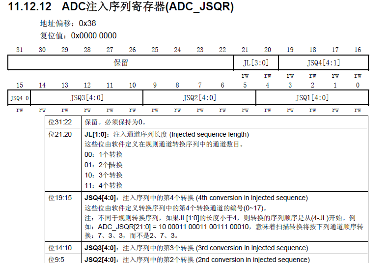
Function: Set the length of the injection channel sequence and the channel number corresponding to each conversion in the sequence (up to 4) .
ADC Injection Data Register x (ADC_JDRx)
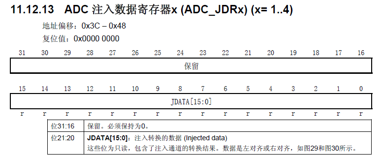
Function: Store the data injected and converted by the ADC.
ADC Rule Data Register (ADC_DR)
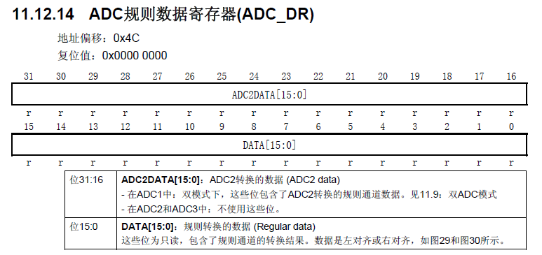
Function: Store the data converted by ADC rules.
ADC Status Register (ADC_SR)

Function: Store various status bits in the ADC conversion process.