Simple test system routine explanation

Based on many years of work experience, the FPGA design process has been summarized in a total of the above 12 steps, some of which can be omitted depending on the difficulty of the project. For example, for very simple projects, we can omit the steps in the dotted box, but our introductory course, no matter how simple it is, will be explained according to these 12 steps.
1. Interpretation of requirements
1.1 Requirements
Use C# to make a host computer interface. Through the asynchronous serial port, you can control the digital tube, LED light, and buzzer on the development board. Press the buttons on the development board at the same time to display which button is currently pressed on the host computer interface. . This experiment is the simplest industrial control equipment with a wide range of applications.
1.2 Knowledge background
Serial port is the abbreviation of "serial interface", that is, an interface that uses serial communication. Serial communication divides data bytes into bits and transmits them one by one on a data line. It is characterized by simple communication lines but slow transmission speed. Therefore, serial ports are widely used in embedded, industrial control and other fields where data transmission speed is not required.
Serial communication is divided into two methods: synchronous serial communication and asynchronous serial communication. Synchronous serial communication requires both communicating parties to transmit data synchronously under the control of the same clock; asynchronous serial communication means that both communicating parties use their own clocks to control the sending and receiving process of data.
UART is a universal asynchronous receiver-transmitter that uses asynchronous serial communication. When sending data, it converts parallel data into serial data for transmission, and when receiving data, it converts the received serial data into serial data. Data is converted into parallel data.
UART serial port communication requires two signal lines, one for serial port transmission and the other for serial port reception. A frame of data during UART transmission or reception consists of 4 parts, start bit, data bit, parity bit and stop bit. The specific timing is shown in Figure 1. Among them, the start bit marks the beginning of a frame of data, the stop bit marks the end of a frame of data, and the data bit is the valid data in a frame of data. The parity bits are divided into odd parity and even parity, which are used to check whether there are errors in the data during transmission. In odd parity, the sender should make the sum of the number of 1s in the data bits and the number of 1s in the check bits an odd number; when the receiver receives the data, it should check the number of 1s. If it is not an odd number, It means that there is an error in the data transmission process. Similarly, even parity checks whether the number of 1's is even.
The data format and transmission rate during UART communication can be set. For correct communication, both the sending and receiving parties should agree on and follow the same settings. The data bits can be selected as 5, 6, 7 or 8 bits, among which 8 data bits are the most commonly used. In practical applications, 8 data bits are generally selected; the parity bit can be odd parity, even parity or none. Check bit; stop bit can be selected from 1 bit (default), 1.5 or 2 bits. The rate of serial communication is represented by the baud rate, which represents the number of binary data transmitted per second, and the unit is bps (bits/second). Commonly used baud rates are 9600, 19200, 38400, 57600, and 115200.
After setting the data format and transmission rate, the UART is responsible for completing the serial-to-parallel conversion of the data, while the signal transmission is implemented by an external drive circuit. The transmission process of electrical signals has different level standards and interface specifications. The interface standards for asynchronous serial communication include RS232, RS422, RS485, etc., which define different electrical characteristics of the interface. For example, RS-232 is a single-ended input and output. RS-422/485 is differential input and output, etc.
The RS232 interface standard appeared earlier and can realize full-duplex working mode, that is, data sending and receiving can be carried out at the same time. When the transmission distance is short (no more than 15m), RS232 is the most commonly used interface standard for serial communication. This chapter mainly introduces UART serial communication for the RS-232 standard.
The most common interface type of the RS-232 standard serial port is DB9, as shown in Figure 2. Industrial computers used in the field of industrial control are generally equipped with multiple serial ports, and many old-fashioned desktop computers are also equipped with serial ports. However, laptops and newer desktop computers do not have serial ports. They generally use USB-to-serial cables (Figure 3) to achieve serial communication with external devices.


The DB9 interface definition and the function description of each pin are shown in Figure 16.1.4. We generally only use pins 2 (RXD), 3 (TXD), and 5 (GND). The other pins are generally used in normal serial port mode. Do not use.

1.3 Hardware design
In this system, we will use basically all the peripherals on the development board. The schematic diagram will not be cut out. You can directly look at the schematic diagram of the development board we provide.
1.4 Interface description
| Signal name | direction | FPGA pin number | illustrate |
|---|---|---|---|
| CLK50M | enter | B10 | Clock signal, 50MHZ |
| FPGA_RX | enter | H14 | Serial signal input |
| FPGA_TX | output | F14 | Serial signal output |
| SMG_W0 | output | E12 | Bit selection control signal, low level can turn on the transistor to power the digital tube bit selection |
| SMG_W1 | output | B15 | Bit selection control signal, low level can turn on the transistor to power the digital tube bit selection |
| SMG_W2 | output | E15 | Bit selection control signal, low level can turn on the transistor to power the digital tube bit selection |
| SMG_W3 | output | H11 | Bit selection control signal, low level can turn on the transistor to power the digital tube bit selection |
| SMG_W4 | output | K16 | Bit selection control signal, low level can turn on the transistor to power the digital tube bit selection |
| SMG_W5 | output | K14 | Bit selection control signal, low level can turn on the transistor to power the digital tube bit selection |
| SMG_A | output | F13 | Digital tube segment selection control signal, low level lights up the segment |
| SMG_B | output | B16 | Digital tube segment selection control signal, low level lights up the segment |
| SMG_C | output | J16 | Digital tube segment selection control signal, low level lights up the segment |
| SMG_D | output | J13 | Digital tube segment selection control signal, low level lights up the segment |
| SMG_E | output | G14 | Digital tube segment selection control signal, low level lights up the segment |
| SMG_F | output | E13 | Digital tube segment selection control signal, low level lights up the segment |
| SMG_G | output | G12 | Digital tube segment selection control signal, low level lights up the segment |
| SMG_DP | output | J14 | Digital tube segment selection control signal, low level lights up the segment |
| KEY1 | output | E4 | Independent button, press low level |
| KEY2 | output | B4 | Independent button, press low level |
| KEY3 | output | C3 | Independent button, press low level |
| KEY4 | output | D3 | Independent button, press low level |
| KEY5 | output | E3 | Independent button, press low level |
| KEY6 | output | H4 | Independent button, press low level |
| LED1 | output | L12 | Connected to LED light, low level LED light turns on |
| LED2 | output | T13 | Connected to LED light, low level LED light turns on |
| LED3 | output | R12 | Connected to LED light, low level LED light turns on |
| LED4 | output | T12 | Connected to LED light, low level LED light turns on |
| LED5 | output | P11 | Connected to LED light, low level LED light turns on |
| LED6 | output | J11 | Connected to LED light, low level LED light turns on |
| LED7 | output | K11 | Connected to LED light, low level LED light turns on |
| LED8 | output | G11 | Connected to LED light, low level LED light turns on |
| BEEP | output | F14 | PWM square wave for driving passive buzzer |
1.5 Communication protocol
In this lesson, we need to make a test system and use the host computer software to control our development board, so we need to formulate a control protocol. This protocol is defined by yourself. Just make sure that the programs of the upper computer and the lower computer are all written according to this protocol, so that you can control it correctly.
- 数码管控制协议-下发(上位机发给下位机)

2.LED灯控制协议-下发(上位机发给下位机)

3.无源蜂鸣器控制协议-下发(上位机发给下位机)

4.按键检测协议-回传(下位机发给上位机)

以上便是我们该项目的通信协议,一个很简单的通信协议,起到抛砖引玉的作用,当控制系统复杂时,我们在定协议的时候需要考虑很多的问题。像我们现在这个简单的控制系统,协议非常简单,仅用于大家学习,便于让大家明白一个控制系统是如何工作的。
2 绘制理论波形图

由于整个工程涉及到的模块较多,理论波形图就不绘制了。但是大家在写程序之前,一定要清楚每个模块内以及模块与模块之间的信号时序关系,这样在仿真出波形时,才能判断出我们当前的程序逻辑是否正确。不然仿真出了波形,也不知道这个波形对不对,那这个项目就没办法完成了。
3 新建TD工程
为了让工程看起来整洁,同时方便工程移植。我们新建4个文件夹,分别是Project,Source,Sim,Doc。
Project — 工程文件夹,里面放的TD工程
Source — 源代码文件夹,里面放的工程源码(.v文件或.vhd文件)
Sim — 仿真文件夹,里面放的仿真相关的文件
Doc — 存放相关资料,比如数据手册,需求文档等
4 编写代码
4.1 按键消抖模块
///
//QQ:3181961725
//TEL/WX:13540738439
//工程师:Mr Wang
//模块介绍:按键消抖模块,主要用来消除按键机械抖动带来的干扰
///
module key_xd(
		input clk,
		input rst_n,
		input key_in,
		output reg	key_out
		);
reg	[3:0] curr_st;
reg	[31:0] wait_cnt;
reg		key_in_ff1;
reg		key_in_ff2;
parameter wait_time=100000;
//for sim
//parameter wait_time=8000;
parameter IDLE=4'd0,
					START=4'd1,
					WAIT=4'd2,
					KEY_VALID=4'd3,
					FINISH=4'd4;
always@(posedge clk)key_in_ff1<=key_in;
always@(posedge clk)key_in_ff2<=key_in_ff1;
always@(posedge clk or negedge rst_n)
	begin
		if(!rst_n)
			curr_st<=IDLE;
		else
			case(curr_st)
				IDLE:
					begin
						if(key_in_ff2==0)
							curr_st<=START;
						else
							;
					end
				START:
					begin
						if(key_in_ff2==1)
							curr_st<=IDLE;
						else if(wait_cnt==wait_time)
							curr_st<=WAIT;
						else
							;
					end
				WAIT:
					begin
						if(key_in_ff2==1)
							curr_st<=IDLE;
						else if(key_in_ff2==0)
							curr_st<=KEY_VALID;
						else
							curr_st<=IDLE;
					end
				KEY_VALID:curr_st<=FINISH;
				FINISH:
					begin
						if(key_in_ff2==1)
							curr_st<=IDLE;
						else
							;
					end
				default:curr_st<=IDLE;
			endcase
	end
	always@(posedge clk or negedge rst_n)
		begin
			if(!rst_n)
				wait_cnt<=0;
			else if(curr_st==START)
				wait_cnt<=wait_cnt+1;
			else
				wait_cnt<=0;
		end
	always@(posedge clk or negedge rst_n)
		begin
			if(!rst_n)
				key_out<=0;
			else if(curr_st==KEY_VALID)
				key_out<=1;
			else
				key_out<=0;
		end
	endmodule
4.2 无源蜂鸣器驱动模块
///
//QQ:3181961725
//TEL/WX:13540738439
//工程师:Mr Wang
//模块介绍:产生PWM波,驱动无源蜂鸣器发声
///
module alarm_ctrl(
	input	clk,
	input	rst_n,
	output	reg	beep
	);
	reg	[15:0]	cnt=0;
	always@(posedge clk or negedge rst_n)begin
		if(!rst_n)
			cnt<=0;
		else if(cnt==10000)
			cnt<=0;
		else
			cnt<=cnt+1;
	end
	always@(posedge clk or negedge rst_n)begin
		if(!rst_n)
			beep<=0;
		else if(cnt==0)
			beep<=~beep;
	end
endmodule
4.3 异步串口接收模块
///
//QQ:3181961725
//TEL/WX:13540738439
//工程师:Mr Wang
//模块介绍:串口接收模块,将串行数据转换成并行数据
///
module async_uart_rev(
	input				rst_n	,//复位信号,低电平有效
	input				clk		,//时钟信号,50MHZ
	input				rxd		,//串行接收数据
	output	reg	[7:0]	rev_data,//并行数据
	output	reg			rev_dvld //并行数据有效标志
	);
	parameter	baud_num=5207;//1/9600*1000000000/20
	parameter	IDLE		=4'd0;
	parameter	START_ST    =4'd1;
	parameter	STOP_ST     =4'd2;
	reg	[12:0]	baud_cnt;
	reg			baud_cnt_en;
	wire		sample_en;
	reg	[3:0]	sample_num;
	reg			rxd_ff1;
	reg			rxd_ff2;
	reg	[3:0]	curr_st;
	always@(posedge clk)rxd_ff2<=rxd_ff1;
	always@(posedge clk)rxd_ff1<=rxd;
	assign	sample_en=(baud_cnt==baud_num[12:1])?1'b1:1'b0;
	//状态机跳转程序
	always@(posedge clk or negedge rst_n)begin
		if(!rst_n)
			curr_st<=IDLE;
		else case(curr_st)
			IDLE:begin
				if(rxd_ff2==0)
					curr_st<=START_ST;
				else;
			end
			START_ST:begin
				if(sample_num==8&&sample_en)
					curr_st<=STOP_ST;
				else;
			end
			STOP_ST:begin
				if(rxd_ff2==1&&sample_en)
					curr_st<=IDLE;
				else;
			end
			default:;
		endcase
	end
	always@(posedge clk or negedge rst_n)begin
		if(!rst_n)
			baud_cnt<=0;
		else if(curr_st==START_ST||curr_st==STOP_ST)begin
			if(baud_cnt==baud_num)
				baud_cnt<=0;
			else
				baud_cnt<=baud_cnt+1;
		end else
			baud_cnt<=0;
	end
	always@(posedge clk or negedge rst_n)begin
		if(!rst_n)
			sample_num<=0;
		else if(sample_en&&sample_num==9)
			sample_num<=0;
		else if(sample_en)
			sample_num<=sample_num+1;
		else;
	end
	always@(posedge clk or negedge rst_n)begin
		if(!rst_n)
			rev_data<=0;
		else if(sample_en)
			case(sample_num)
			1:rev_data[0]<=rxd_ff2;
			2:rev_data[1]<=rxd_ff2;
			3:rev_data[2]<=rxd_ff2;
			4:rev_data[3]<=rxd_ff2;
			5:rev_data[4]<=rxd_ff2;
			6:rev_data[5]<=rxd_ff2;
			7:rev_data[6]<=rxd_ff2;
			8:rev_data[7]<=rxd_ff2;
			default:;
		endcase
	end
	always@(posedge clk or negedge rst_n)begin
		if(!rst_n)
			rev_dvld<=0;
		else if(sample_num==9&&sample_en)
			rev_dvld<=1;
		else
			rev_dvld<=0;
	end
endmodule
4.4 异步串口发送模块
///
//QQ:3181961725
//TEL/WX:13540738439
//工程师:Mr Wang
//模块介绍:串口发送模块,将并行数据转换成串行数据
///
module async_uart_tran(
	input			rst_n		,//复位信号,低电平有效
	input			clk			,//时钟,50MHZ
	input	[7:0]	tran_data	,//输入的并行数据
	input			tran_dvld	,//输入的并行数据有效标志
	output	reg		txd          ,//串行输出数据
	output			byte_txfini
	);
	parameter	baud_num=5207;//1/9600*1000000000/20
	parameter	IDLE		=4'd0;
	parameter	DATA_ST    =4'd1;
	parameter	START_ST    =4'd2;
	parameter	STOP_ST     =4'd3;
	reg	[12:0]	baud_cnt;
	reg			baud_cnt_en;
	wire		sample_en;
	reg	[3:0]	sample_num;
	reg	[3:0]	curr_st;
	assign	byte_txfini=(curr_st==STOP_ST&&sample_en)?1'b1:1'b0;
	assign	sample_en=(baud_cnt==baud_num)?1'b1:1'b0;
	always@(posedge clk or negedge rst_n)begin
		if(!rst_n)
			curr_st<=IDLE;
		else case(curr_st)
			IDLE:begin
				if(tran_dvld==1)
					curr_st<=START_ST;
				else;
			end
			START_ST:begin
				if(sample_en==1)
					curr_st<=DATA_ST;
			end
			DATA_ST:begin
				if(sample_en&&sample_num==8)
					curr_st<=STOP_ST;
				else;
			end
			STOP_ST:begin
				if(sample_en==1)
					curr_st<=IDLE;
				else;
			end
			default:;
		endcase
	end
	always@(posedge clk or negedge rst_n)begin
		if(!rst_n)
			baud_cnt<=0;
		else if(curr_st==START_ST||curr_st==DATA_ST||curr_st==STOP_ST)begin
			if(baud_cnt==baud_num)
				baud_cnt<=0;
			else
				baud_cnt<=baud_cnt+1;
		end else
			baud_cnt<=0;
	end
	always@(posedge clk or negedge rst_n)begin
		if(!rst_n)
			sample_num<=0;
		else if(curr_st==IDLE)
			sample_num<=0;
		else if(sample_en)
			sample_num<=sample_num+1;
		else;
	end
	always@(posedge clk or negedge rst_n)begin
		if(!rst_n)
			txd<=1;
		else if(sample_en)
			case(sample_num)
			0:txd<=1'b0;
			1:txd<=tran_data[0];
			2:txd<=tran_data[1];
			3:txd<=tran_data[2];
			4:txd<=tran_data[3];
			5:txd<=tran_data[4];
			6:txd<=tran_data[5];
			7:txd<=tran_data[6];
			8:txd<=tran_data[7];
			9:txd<=1'b1;
			default:txd<=1;
		endcase
	end
endmodule
4.5 指令解析模块
///
//QQ:3181961725
//TEL/WX:13540738439
//工程师:Mr Wang
//模块介绍:将收到的指令按协议解析出来,分别控制数码管,LED灯和蜂鸣器模块
///
module cmd_ctrl(
	input				clk,
	input				rst_n,
	input				rev_dvld,
	input		[7:0]	rev_data,
	output	reg	[3:0]	smg_00,
	output	reg	[3:0]	smg_01,
	output	reg	[3:0]	smg_02,
	output	reg	[3:0]	smg_03,
	output	reg	[3:0]	smg_04,
	output	reg	[3:0]	smg_05,
	output	reg	[7:0]	led,
	output	reg			beep
	);
	parameter	IDLE		=4'd0;
	parameter	CMD0_ST	    =4'd1;
	parameter	SMG00_ST    =4'd2;
	parameter	SMG01_ST    =4'd3;
	parameter	SMG02_ST    =4'd4;
	parameter	SMG03_ST    =4'd5;
	parameter	SMG04_ST    =4'd6;
	parameter	SMG05_ST    =4'd7;
	parameter	LED_ST      =4'd8;
	parameter	ALARM_ST    =4'd9;
	reg	[3:0]	curr_st;
	always@(posedge clk or negedge rst_n)begin
		if(!rst_n)begin
			curr_st<=IDLE;
		end else case(curr_st)
			IDLE:begin
				if(rev_dvld&&rev_data==8'haa)
					curr_st<=CMD0_ST;
				else;
			end
			CMD0_ST:begin
				if(rev_dvld&&rev_data==8'h00)//数码管
					curr_st<=SMG00_ST;
				else if(rev_dvld&&rev_data==8'h01)//LED灯
					curr_st<=LED_ST;
				else if(rev_dvld&&rev_data==8'h02)//蜂鸣器
					curr_st<=ALARM_ST;
				else;
			end
			SMG00_ST:begin
				if(rev_dvld)
					curr_st<=SMG01_ST;
				else;
			end
			SMG01_ST:begin
				if(rev_dvld)
					curr_st<=SMG02_ST;
				else;
			end
			SMG02_ST:begin
				if(rev_dvld)
					curr_st<=SMG03_ST;
				else;
			end
			SMG03_ST:begin
				if(rev_dvld)
					curr_st<=SMG04_ST;
				else;
			end
			SMG04_ST:begin
				if(rev_dvld)
					curr_st<=SMG05_ST;
				else;
			end
			SMG05_ST:begin
				if(rev_dvld)
					curr_st<=IDLE;
				else;
			end
			LED_ST:begin
				if(rev_dvld)
					curr_st<=IDLE;
				else;
			end
			ALARM_ST:begin
				if(rev_dvld)
					curr_st<=IDLE;
				else;
			end
			default:;
		endcase
	end
	always@(posedge clk or negedge rst_n)begin
		if(!rst_n)begin
			smg_00	<=0;
			smg_01	<=0;
			smg_02	<=0;
			smg_03	<=0;
			smg_04	<=0;
			smg_05	<=0;
		end else if(curr_st==SMG00_ST)begin
			smg_00<=rev_data;
		end else if(curr_st==SMG01_ST)begin
			smg_01<=rev_data;
		end else if(curr_st==SMG02_ST)begin
			smg_02<=rev_data;
		end else if(curr_st==SMG03_ST)begin
			smg_03<=rev_data;
		end else if(curr_st==SMG04_ST)begin
			smg_04<=rev_data;
		end else if(curr_st==SMG05_ST)begin
			smg_05<=rev_data;
		end else;
	end
	always@(posedge clk or negedge rst_n)begin
		if(!rst_n)begin
			led<=8'hff;
		end else if(curr_st==LED_ST)
			led<=rev_data;
		else;
	end
	always@(posedge clk or negedge rst_n)begin
		if(!rst_n)
			beep<=0;
		else if(curr_st==ALARM_ST)
			beep<=rev_data[0];
		else;
	end
endmodule
4.6 通信协议生成模块
///
//QQ:3181961725
//TEL/WX:13540738439
//工程师:Mr Wang
//模块介绍:生成按键检测的通信协议
///
`timescale 1ns/1ps
module uart_data_gen(
	input				clk,
	input				rst_n,
	input				key0,
	input				key1,
	input				key2,
	input				key3,
	input				key4,
	input				key5,
	input				byte_end,
	output	reg	[ 7:0]	data,
	output	reg			data_valid
	);
parameter 	idle  			= 8'd0;
parameter 	word1 			= 8'd1;
parameter	word1_gap		= 8'd2;

reg	[ 7:0] 	curr_st	;
reg	[ 7:0] 	word_cnt	;
reg	[ 7:0]	title		;
reg			byte_end_ff1;
wire		byte_end_rise;
wire[7:0]	data_tmp	;
assign	byte_end_rise=byte_end&(!byte_end_ff1);
always@(posedge clk)byte_end_ff1<=byte_end;
always@(posedge clk or negedge rst_n)
	begin
		if(!rst_n)
			title<=8'hff;
		else if(key0)
			title<=8'h00;
		else if(key1)
			title<=8'h01;
		else if(key2)
			title<=8'h02;
		else if(key3)
			title<=8'h03;
		else if(key4)
			title<=8'h04;
		else if(key5)
			title<=8'h05;
		else;
	end
always@(posedge clk or negedge rst_n)
	begin
		if(!rst_n)
			curr_st<=idle;
		else case(curr_st)
			idle:
				begin
					if(key0||key1||key2||key3||key4||key5)
						curr_st<=word1;
					else
						;
				end
			word1:
				begin
					if(word_cnt==2)
						curr_st<=word1_gap;
					else
						;
				end
			word1_gap:curr_st<=idle;
			default:;
		endcase
	end
always@(posedge clk or negedge rst_n)
	begin
		if(!rst_n)
			word_cnt<=0;
		else if(curr_st==idle||curr_st==word1_gap)
			word_cnt<=0;
		else if((curr_st==word1)&byte_end)
			word_cnt<=word_cnt+1;
		else
			;
	end
always@(posedge clk or negedge rst_n)
	begin
		if(!rst_n)
			begin
				data<=0;
				data_valid<=0;
			end
		else case({curr_st,word_cnt})

			{word1,8'h0}:begin data<=8'haa ;data_valid<=1;end
			{word1,8'h1}:begin data<=title;data_valid<=1;end
			default:  begin data<=8'h00;data_valid<=0;end
		endcase
	end
endmodule
4.7 数码管显示模块
///
//QQ:3181961725
//TEL/WX:13540738439
//工程师:Mr Wang
//模块介绍:数码管动态扫描
///
module smg(
	input				clk		,//时钟
	input				rst_n	,//复位,低电平有效
	input		[3:0] 	swan	,//十万位数
	input		[3:0] 	wan		,//万位数
	input		[3:0] 	qian	,//千位数
	input		[3:0] 	bai		,//百位数
	input		[3:0] 	shi		,//十位数
	input		[3:0] 	ge		,//个位数
	output 	reg	[5:0]	sm_bit	,//数码管选择输出引脚
	output 	reg	[7:0] 	sm_seg	 //数码管段输出引脚
	);

	reg	[ 3:0]	disp_dat;//定义显示数据寄存器
	reg	[24:0]	count	;//定义计数寄存器
//扫描信号产生部分
always @(posedge clk or negedge rst_n)//定义clock上升沿触发
begin
	if(!rst_n)
		count<=0;
	else if(count == 25'd250000)
		count <= 25'd0;						//计数器清零
	else
		count <= count + 1'b1;
end
//数码管动态扫描显示部分
always @(posedge clk or negedge rst_n)
begin
	if(!rst_n)
		disp_dat<=0;
	else case(count[15:13])//选择扫描显示数据
		3'd0:disp_dat <= ge		;//个位
		3'd1:disp_dat <= shi	;//十位
		3'd2:disp_dat <= bai	;//百位
		3'd3:disp_dat <= qian	;//千位
		3'd4:disp_dat <= wan	;//万位
		3'd5:disp_dat <= swan	;//十万位
	endcase
end
always @(posedge clk)
begin
	case(count[15:13])			 //选择扫描显示数据
		3'd0:sm_bit <= 6'b111110;//选择第一个数码管显示
		3'd1:sm_bit <= 6'b111101;//选择第二个数码管显示
		3'd2:sm_bit <= 6'b111011;//选择第三个数码管显示
		3'd3:sm_bit <= 6'b110111;//选择第四个数码管显示
		3'd4:sm_bit <= 6'b101111;//选择第五个数码管显示
		3'd5:sm_bit <= 6'b011111;//选择第六个数码管显示
	endcase
end
always @(posedge clk)
begin
	case(disp_dat)
		4'h0:sm_seg <= 8'hc0;	//显示0
		4'h1:sm_seg <= 8'hf9;	//显示1
		4'h2:sm_seg <= 8'ha4;	//显示2
		4'h3:sm_seg <= 8'hb0;	//显示3
		4'h4:sm_seg <= 8'h99;	//显示4
		4'h5:sm_seg <= 8'h92;	//显示5
		4'h6:sm_seg <= 8'h82;	//显示6
		4'h7:sm_seg <= 8'hf8;	//显示7
		4'h8:sm_seg <= 8'h80;	//显示8
		4'h9:sm_seg <= 8'h90;	//显示9
		4'ha:sm_seg <= 8'hbf;	//显示-
		default:sm_seg <= 8'hff;//不显示
	endcase
end
endmodule
4.8 顶层模块
///
//QQ:3181961725
//TEL/WX:13540738439
//工程师:Mr Wang
//模块介绍:顶层模块,例化各个功能模块,使工程看起来整洁清晰
///
module ctrl_system_top(
	input			clk			,
	input			rst_n		,
	input	[5:0]	key			,
	input			uart_rxd	,
	output			uart_txd	,
	output	[5:0]	sm_bit		,
	output	[7:0]	sm_seg		,
	output	[7:0]	led			,
	output			alarm
	);
wire	[7:0]	rev_data;
wire 	[3:0]	smg_00	;
wire 	[3:0]	smg_01  ;
wire 	[3:0]	smg_02  ;
wire 	[3:0]	smg_03  ;
wire 	[3:0]	smg_04  ;
wire 	[3:0]	smg_05  ;
wire	[7:0]	tran_data;
wire			beep;
wire			beep_en;
wire			key0_out,key1_out,key2_out,key3_out,key4_out,key5_out;
assign	alarm=(beep_en)?beep:1'b1;
key_xd Ukey_xd0(
	.clk	(clk		),
	.rst_n	(rst_n		),
	.key_in	(key[0]		),
	.key_out(key0_out	)
	);
key_xd Ukey_xd1(
	.clk	(clk		),
	.rst_n	(rst_n		),
	.key_in	(key[1]		),
	.key_out(key1_out	)
	);
key_xd Ukey_xd2(
	.clk	(clk		),
	.rst_n	(rst_n		),
	.key_in	(key[2]		),
	.key_out(key2_out	)
	);
key_xd Ukey_xd3(
	.clk	(clk		),
	.rst_n	(rst_n		),
	.key_in	(key[3]		),
	.key_out(key3_out	)
	);
key_xd Ukey_xd4(
	.clk	(clk		),
	.rst_n	(rst_n		),
	.key_in	(key[4]		),
	.key_out(key4_out	)
	);
key_xd Ukey_xd5(
	.clk	(clk		),
	.rst_n	(rst_n		),
	.key_in	(key[5]		),
	.key_out(key5_out	)
	);
async_uart_rev Uasync_uart_rev(
	.rst_n		(rst_n),
	.clk		(clk),
	.rxd		(uart_rxd),
	.rev_data	(rev_data),
	.rev_dvld   (rev_dvld)
	);
cmd_ctrl Ucmd_ctrl(
	.clk		(clk		),
	.rst_n		(rst_n		),
	.rev_dvld	(rev_dvld	),
	.rev_data	(rev_data	),
	.smg_00		(smg_00		),
	.smg_01		(smg_01		),
	.smg_02		(smg_02		),
	.smg_03		(smg_03		),
	.smg_04		(smg_04		),
	.smg_05		(smg_05		),
	.led		(led		),
	.beep       (beep_en    )
	);
smg Usmg(
	.clk		(clk		),//时钟
	.rst_n		(rst_n		),//复位,低电平有效
	.swan		(smg_00		),//十万位数
	.wan		(smg_01		),//万位数
	.qian		(smg_02		),//千位数
	.bai		(smg_03		),//百位数
	.shi		(smg_04		),//十位数
	.ge			(smg_05		),//个位数
	.sm_bit		(sm_bit		),//数码管选择输出引脚
	.sm_seg	 	(sm_seg		)//数码管段输出引脚
	);
alarm_ctrl Ualarm_ctrl(
	.clk		(clk),
	.rst_n		(rst_n),
	.beep       (beep)
	);
uart_data_gen Uuart_data_gen(
	.clk		(clk),
	.rst_n		(rst_n),
	.key0		(key0_out),
	.key1		(key1_out),
	.key2		(key2_out),
	.key3		(key3_out),
	.key4		(key4_out),
	.key5		(key5_out),
	.byte_end	(byte_txfini),
	.data		(tran_data),
	.data_valid (tran_dvld)
	);
async_uart_tran Uasync_uart_tran(
	.rst_n		(rst_n),//复位信号,低电平有效
	.clk		(clk),//时钟,50MHZ
	.tran_data	(tran_data),//输入的并行数据
	.tran_dvld	(tran_dvld),//输入的并行数据有效标志
	.txd        (uart_txd), //串行输出数据
	.byte_txfini(byte_txfini)
	);
endmodule
5. 编写仿真测试激励文件
我们知道,写仿真激励文件时,只关心输入信号,在该项目中,输入信号有clk,rst_n,key[5:0],uart_rxd,所以我们只需要在TB文件里对这几个信号操作即可。clk,rst_n,key[5:0],这几个信号的激励比较简单,在上几讲里都有涉及到,只是uart_rxd这个信号的激励相对来说要麻烦一些。因为,我们必须按异步串口通信的协议给这个uart_rxd赋值,相当于我们在TB文件里面要写一个串口发送模块,这样才能产生一个正确的uart_rxd激励信号。
5.1 顶层仿真文件
`timescale 1ns/1ns
module async_uart_top_tb;
	reg					clk		;
	reg					rst_n	;
	reg	[5:0]			key		;
	wire				rxd		;
	reg	[17:0]			cnt=0;
	wire[7:0]			tran_data;
initial
begin
	clk = 0;
	rst_n=0;
	key=6'h3f;
	#1000
	rst_n=1;
end
always #10 clk=~clk;
always@(posedge clk)cnt<=cnt+1;
always@(posedge clk)begin
	if(cnt>10000&&cnt<20000)//按下KEY1
		key<=6'b111110;
	else
		key<=6'b111111;
end
//生成通信协议数据
uart_data_gen_sim Uuart_data_gen_sim(
	.clk		(clk		),
	.rst_n		(rst_n		),
	.byte_end	(byte_txfini),
	.data		(tran_data	),
	.data_valid (tran_dvld	)
	);
//将通信协议以串口的形式发送出去
async_uart_tran Uasync_uart_tran(
	.rst_n		(rst_n		),
	.clk		(clk		),
	.tran_data	(tran_data	),
	.tran_dvld	(tran_dvld	),
	.txd        (rxd		),
	.byte_txfini(byte_txfini)
	);
//被仿真的工程顶层文件
ctrl_system_top Uctrl_system_top(
	.clk			(clk	),
	.rst_n			(rst_n	),
	.key			(key	),
	.uart_rxd		(rxd	),
	.uart_txd		(),
	.sm_bit			(),
	.sm_seg			(),
	.led			(),
	.alarm          ()
	);
endmodule
5.2 通信协议生成模块
该模块主要用于生成数码管控制协议,LED灯控制协议和蜂鸣器控制协议,在我们仿真时,一次只能仿真一个控制协议,如果我们仿真数码管控制协议就需要在程序中注释掉LED灯控制协议和蜂鸣器控制协议。
`timescale 1ns/1ps
module uart_data_gen_sim(
	input				clk,
	input				rst_n,
	input				byte_end,
	output	reg	[ 7:0]	data,
	output	reg			data_valid
	);
parameter 	idle  			= 8'd0;
parameter 	word1 			= 8'd1;
parameter	word1_gap		= 8'd2;
parameter	word_num		=8;//控制数码管的协议为8个字节
//parameter	word_num		=3;//控制LED灯和蜂鸣器的协议为3个字节
reg	[ 7:0] 	curr_st	;
reg	[ 7:0] 	word_cnt	;
reg	[ 7:0]	title		;
reg			byte_end_ff1;
wire		byte_end_rise;
wire[7:0]	data_tmp	;
assign	byte_end_rise=byte_end&(!byte_end_ff1);
always@(posedge clk)byte_end_ff1<=byte_end;
always@(posedge clk or negedge rst_n)
	begin
		if(!rst_n)
			curr_st<=idle;
		else case(curr_st)
			idle:curr_st<=word1;
			word1:
				begin
					if(word_cnt==word_num)
						curr_st<=word1_gap;
					else
						;
				end
			word1_gap:;//curr_st<=idle;
			default:;
		endcase
	end
always@(posedge clk or negedge rst_n)
	begin
		if(!rst_n)
			word_cnt<=0;
		else if(curr_st==idle||curr_st==word1_gap)
			word_cnt<=0;
		else if((curr_st==word1)&byte_end)
			word_cnt<=word_cnt+1;
		else
			;
	end
always@(posedge clk or negedge rst_n)
	begin
		if(!rst_n)
			begin
				data<=0;
				data_valid<=0;
			end
		else case({curr_st,word_cnt})
		    /控制数码管/
			{word1,8'h0}:begin data<=8'haa;data_valid<=1;end
			{word1,8'h1}:begin data<=8'h00;data_valid<=1;end
			{word1,8'h2}:begin data<=8'h01;data_valid<=1;end//第一位数码管显示的值
			{word1,8'h3}:begin data<=8'h02;data_valid<=1;end//第二位数码管显示的值
			{word1,8'h4}:begin data<=8'h03;data_valid<=1;end//第三位数码管显示的值
			{word1,8'h5}:begin data<=8'h04;data_valid<=1;end//第四位数码管显示的值
			{word1,8'h6}:begin data<=8'h05;data_valid<=1;end//第五位数码管显示的值
			{word1,8'h7}:begin data<=8'h06;data_valid<=1;end//第六位数码管显示的值
			/控制LED灯/
			// {word1,8'h0}:begin data<=8'haa;data_valid<=1;end
			// {word1,8'h1}:begin data<=8'h01;data_valid<=1;end
			// {word1,8'h2}:begin data<=8'hfe;data_valid<=1;end//点亮第一个LED灯
			/控制蜂鸣器/
			// {word1,8'h0}:begin data<=8'haa;data_valid<=1;end
			// {word1,8'h1}:begin data<=8'h02;data_valid<=1;end
			// {word1,8'h2}:begin data<=8'h01;data_valid<=1;end//打开蜂鸣器
			default:  begin data<=8'h00;data_valid<=0;end
		endcase
	end
endmodule
6. Modelsim仿真
Modelsim仿真一般有两种方法,第一种是图形化界面仿真,即所有的操作都是在Modelsim软件界面上来完成,该方式的优点是,简单易学,适用于简单的项目,缺点是操作步骤繁琐。第二种是批处理仿真,这种方式在仿真前需要编写相应的脚本文件,该方式的优点是,一键即可完成仿真,省时省力,缺点是前期需要编写脚本文件。为了更贴近工程实际,从第三课开始采用批处理的方式进行仿真。
6.1 数码管控制仿真波形如下:

通过上面的仿真波形我们可以看到,smg_00等于1,smg_01等于2…smg_05等于6,在通信协议生成模块(uart_data_gen_sim.v)中,我们给数码管赋值也是123456,仿真结果与设计相符,逻辑功能正确。
6.2 LED灯控制

通过上面的仿真波形我们可以看到,led等于8’b11111110,在通信协议生成模块(uart_data_gen_sim.v)中,我们给LED灯赋值也是8’b11111110,仿真结果与设计相符,逻辑功能正确。
6.3 蜂鸣器控制

From the above simulation waveform, we can see that alarm outputs a PWM square wave signal. In the communication protocol generation module (uart_data_gen_sim.v), we assign a value to the buzzer of 8'h01, that is, turn on the buzzer, and the simulation result is also I saw that there is a PWM signal output, which is consistent with the design and the logic function is correct.
7. Compare waveforms
Since we did not draw the theoretical waveform, we only need to ensure that there is no problem with the simulated waveform during simulation.
8 Add .v file

9 Bind the pins and save the constraint file (.adc)


10 Compile and synthesize the BIT file

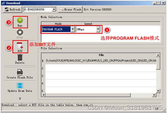
11. Download BIT file


After the download is successful, you can communicate with our host computer test software. The specific steps are as follows
1) Install the serial port driver
2) Connect one end of the power cord to the USB interface of the computer and the other end to the power supply port of the development board
3) Download the FPGA program
4 ) Open the "Development Board Test Platform.exe" executable file
5) If the serial port driver is installed successfully, the host computer will automatically identify the port number, select 9600 for the baud rate, and then open the connection, as shown below:

6) After the connection is successful, you can proceed Controlled by the development board, you can change the numbers displayed on the digital tube. After setting, click the setting button, and the development board will display the numbers set by the host computer.

7) Press the button on the development board to display the currently pressed button, as shown below :

8) During LED light control, when the LED on the development board is turned on, the corresponding button will turn red, indicating that the corresponding LED light is turned on. As shown in the figure below, LED0, LED2, and LED4 are lit.

9) Press the buzzer button and the buzzer will alarm. Press it again and the alarm will turn off.
If there are no problems with the above tests, it means that our program is OK and the program can be solidified.
12 solidification configuration file
FPGA has a characteristic that the configuration information will be lost after power failure, so we need to store the configuration information in the configuration chip (FLASH). After the development board is powered on, the FPGA will read the configuration information in the configuration chip, so the development The board can still work normally after powering off and on again.
After the curing is successful, power off the development board and then power it on again. It can be observed that the development board can still perform the functions just now.