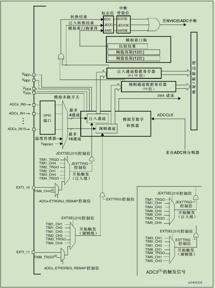
ADC (analog signal to digital signal) is still used in embedded applications. The signals collected on many sensors are analog signals (common temperature and light-sensitive sensors). Because analog signals are not good enough, they are often converted into Numerical signal for easy identification. The ADC converter in M3 is 12-bit precision with up to 18 channels (16 external channels + 2 internal signal sources). The A / D conversion of each channel can be performed in single, continuous, scan or discontinuous mode, and each The sampling time can be set separately for each channel, and the ADC conversion result can also be stored in the 16-bit data register in a left-aligned or right-aligned manner. And the M3 ADC also supports analog watchdog to allow the application to detect whether the input voltage exceeds the user-defined high / low threshold, and an interrupt can be generated if it exceeds.Note that the input clock of the ADC must not exceed 14MHz, the power supply of the ADC is between 2.4-3.6V, and the measurement range of the ADC voltage is V ref + -V ref- .
ADC Framework
-
ADCx_INx: analog input signal, 16 external analog input channels.
-
V ref + , V ref- : Analog reference positive and negative. The high-side / positive reference voltage used by the ADC is 2.4V ≤ V REF + ≤ V DDA .
-
V DDA , V SSA : ADC analog power supply, used to power the ADC module.
-
ADC switch control.
After M3 is powered on, in order to reduce the power consumption of the device, the clocks of the peripherals are basically turned off, so it is necessary to turn on the clock of the ADC module before using the ADC. The maximum input clock of the ADC module is 14M . The RCC controller provides a dedicated programmable prescaler for the ADC. The library functions are:
void RCC_APB2PeriphResetCmd(uint32_t RCC_APB2Periph, FunctionalState NewState)
	 RCC_APB2PeriphResetCmd	(RCC_APB2Periph_ADC1,ENABLE);
/**
  * @brief  Configures the ADC clock (ADCCLK).
  * @param  RCC_PCLK2: defines the ADC clock divider. This clock is derived from
  *   the APB2 clock (PCLK2).
  *   This parameter can be one of the following values:
  *     @arg RCC_PCLK2_Div2: ADC clock = PCLK2/2
  *     @arg RCC_PCLK2_Div4: ADC clock = PCLK2/4
  *     @arg RCC_PCLK2_Div6: ADC clock = PCLK2/6
  *     @arg RCC_PCLK2_Div8: ADC clock = PCLK2/8
  * @retval None
  */
void RCC_ADCCLKConfig(uint32_t RCC_PCLK2)
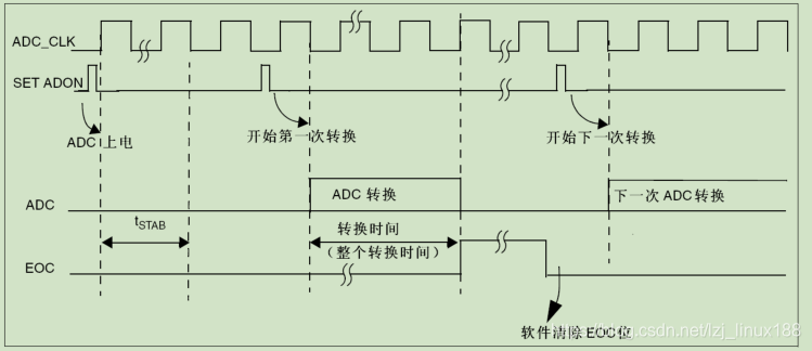
After the ADC clock is turned on, the ADC enters the power-down mode (low power consumption), you need to set the ADON bit of the configuration register to wake it up, and it takes a delay (S STAB ) to stabilize the ADC module after the ADC wakes up. Will be replaced. ** You can stop the conversion by clearing the ADON bit and put the ADC in power-down mode. ** The ADC needs a stabilization time t STAB before starting the precision conversion , which is used to stabilize the ADC module, set ADON to trigger the conversion, and the converted data is stored in the corresponding data register.
The library functions to enable the ADC module are:
/*唤醒ADC模块*/
 /*@brief  Enables or disables the specified ADC peripheral.*/
void ADC_Cmd(ADC_TypeDef* ADCx, FunctionalState NewState);
- Analog watchdog The
register can be set to enable the function of analog watchdog. The analog watchdog can function on one or more channels (need to configure AWDSGL, AWDEN, JAWDEN). When the voltage is not between the high and low thresholds, an interrupt will be generated. ADC_HTR and ADC_LTR are registers that configure high and low thresholds, and AWDIE interrupt enable bit.

Corresponding library function:
/**
  * @brief  Enables or disables the analog watchdog on single/all regular
  *         or injected channels
  * @param  ADCx: where x can be 1, 2 or 3 to select the ADC peripheral.
  * @param  ADC_AnalogWatchdog: the ADC analog watchdog configuration.
  *   This parameter can be one of the following values:
  *     @arg ADC_AnalogWatchdog_SingleRegEnable: Analog watchdog on a single regular channel
  *     @arg ADC_AnalogWatchdog_SingleInjecEnable: Analog watchdog on a single injected channel
  *     @arg ADC_AnalogWatchdog_SingleRegOrInjecEnable: Analog watchdog on a single regular or injected channel
  *     @arg ADC_AnalogWatchdog_AllRegEnable: Analog watchdog on  all regular channel
  *     @arg ADC_AnalogWatchdog_AllInjecEnable: Analog watchdog on  all injected channel
  *     @arg ADC_AnalogWatchdog_AllRegAllInjecEnable: Analog watchdog on all regular and injected channels
  *     @arg ADC_AnalogWatchdog_None: No channel guarded by the analog watchdog
  * @retval None
  */
void ADC_AnalogWatchdogCmd(ADC_TypeDef* ADCx, uint32_t ADC_AnalogWatchdog);/*开启模拟看门狗*/
void ADC_AnalogWatchdogThresholdsConfig(ADC_TypeDef* ADCx, uint16_t HighThreshold, uint16_t LowThreshold);/*设置模拟看门狗的高低阀值*/
void ADC_AnalogWatchdogSingleChannelConfig(ADC_TypeDef* ADCx, uint8_t ADC_Channel);/*假如模拟看门狗是单通道使用,则需要指定哪个通道使用模拟看门狗*/
- Channel sampling time The channel sampling time
can be set by the SMP [2: 0] bits in the configuration register, each channel is independent. Replacement time T CONV = sampling time + 12.5 cycles. - Channel selection
Combine the conversion groups in any order on any number of channels. The rule group can be composed of up to 16 sequences, and the conversion order is configured in ADC_SQRx; while the injection group consists of up to 4 conversion sequences, the conversion order is stored in ADC_JSQR. If the sequence is modified during the conversion, the current conversion will be cleared, and
the library function corresponding to the newly selected group will be converted.
/*此函数用于设置规则组通道序列以及采样的时间,*/
void ADC_RegularChannelConfig(ADC_TypeDef* ADCx, uint8_t ADC_Channel, uint8_t Rank, uint8_t ADC_SampleTime);
- Data storage.
The ALIGN bit in the ADC configuration register can set the alignment of the converted data. You can select left or right alignment. The converted data of the injected channel will be stored in the ADC injection data register; the converted data of the regular channel will be stored in the lower 16 bits of the ADC regular data register. If the DMA function is enabled, a DMA interrupt will be generated to transfer the data to the specified SRAM location. There is only one data register in the rule group, so there will be coverage problems during scanning or continuous conversion, so you need to use the DMA function; and each channel in the injection group corresponds to a data register, without using the DMA function. The
corresponding library function:
uint16_t ADC_GetConversionValue(ADC_TypeDef* ADCx);/*获取规则组数据寄存器值*/
uint16_t ADC_GetInjectedConversionValue(ADC_TypeDef* ADCx, uint8_t ADC_InjectedChannel);/*获取注入组数据寄存器值*/
/**
  * @brief  Enables or disables the specified ADC DMA request.
  * @param  ADCx: where x can be 1 or 3 to select the ADC peripheral.
  *   Note: ADC2 hasn't a DMA capability.
  * @param  NewState: new state of the selected ADC DMA transfer.
  *   This parameter can be: ENABLE or DISABLE.
  * @retval None
  */
void ADC_DMACmd(ADC_TypeDef* ADCx, FunctionalState NewState);/*开启DMA功能*/
- ADC conversion mode.
Single conversion mode : ADC only performs one conversion.It can be started by setting the ADON bit in the register (only applicable to regular channels) or can be triggered by the channel external trigger, At this time the CONT bit is 0. The conversion end EOC flag is set to ADC to stop.
Continuous conversion mode : start another conversion as soon as the previous ADC conversion is completed.Can be started by external trigger or set ADON bit, At this time the CONT bit is 1. After the conversion of each channel is completed, the conversion end flag (<J> EOC) is set to the
scan mode : SCAN of the register can be configured to enable it. The ADC will scan all channels selected by the ADC_SQRx register or ADC_JSQR. At the end of the replacement of each channel of each group, the next channel will be automatically converted. If it is configured for continuous conversion at the same time, the ADC always converts cyclically. Each channel conversion end The conversion end flag will be set to a
discontinuous mode : it can be used to perform a short sequence of conversions. The conversion channel is part of the conversion sequence group selected by the ADC_SQRx register or ADC_JSQR. After the conversion trigger signal is generated, a round of conversion will be performed until all channels in the short sequence are converted, and the conversion sequence will not automatically start from the beginning . The rule group converts up to 8 channels at a time, and the injection group converts up to 4 channels at a time. The discontinuous mode can only be used for group conversion, and the injection group cannot use automatic injection and discontinuous mode at the same time.External event trigger
Trigger injection : Clear JAUTO and set the JSWSTART bit to trigger the injection conversion function.At this time, if there is a regular channel conversion, it is suspended. The injection channel sequence is converted by a single scan. Then resume the rule group channel conversion that was interrupted last time. Equivalent to the priority of injection conversion is higher than the rule group
Automatic injection can also be triggered by an external JSWSTART event : Set the JAUTO bit of the register, and the injection group channel is automatically converted.This mode must prohibit the external trigger conversion function, Can be used to convert up to 20 conversion sequences set in the ADC_SQRx and ADC_JSQR registers . This mode can also be configured for continuous conversion mode .
After the replacement, the data will be stored in the corresponding data register, the EOC flag is set, if the interrupt is enabled, a corresponding interrupt will be generated.
Since there is only one rule group data register, there will be data coverage during continuous conversion. Here you can set the DMA bit in the configuration register. After each conversion, the DMA transfers the data in the data register to the SRAM; The data of channel replacement is always stored in ADC_JDRx, and each injection channel has a corresponding data register to save the data.
/*开始转换规则通道,软件设置硬件清除*/
void ADC_SoftwareStartConvCmd(ADC_TypeDef* ADCx, FunctionalState NewState);
FlagStatus ADC_GetSoftwareStartConvStatus(ADC_TypeDef* ADCx);
/*配置和使能间断模式*/
void ADC_DiscModeChannelCountConfig(ADC_TypeDef* ADCx, uint8_t Number);
void ADC_DiscModeCmd(ADC_TypeDef* ADCx, FunctionalState NewState);
/*规则组的外部触发使能,触发方式在ADC_InitTypeDef->ADC_ExternalTrigConv指定*/
void ADC_ExternalTrigConvCmd(ADC_TypeDef* ADCx, FunctionalState NewState);
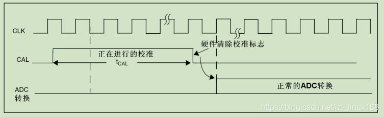
- Calibration
ADC has a built-in self-calibration mode. Calibration can greatly reduce the quasi-accuracy error caused by changes in the internal capacitor bank. During calibration, an error correction code (digital value) is calculated on each capacitor, and this code is used to eliminate the error generated on each capacitor in the subsequent conversion.
Start the calibration by setting the CAL bit in the ADC_CR2 register. Once the calibration is completed, the CAL bit is reset by the hardware and normal conversion can begin. It is recommended to perform an ADC calibration at power-up. After the calibration phase, the calibration code is stored in ADC_DR. M3 self-calibration, you can get the value of the data register directly after the conversion
It is recommended to perform a calibration after each power-on. Before starting the calibration, the ADC must be in the power-off state (ADON) for more than two ADC clock cycles
The corresponding library functions are:
/*RSTCAL:复位校准和CAL:A/D校准都是由软件设置硬件清除,校准时ADC要处于关电状态*/
void ADC_ResetCalibration(ADC_TypeDef* ADCx);
FlagStatus ADC_GetResetCalibrationStatus(ADC_TypeDef* ADCx);
void ADC_StartCalibration(ADC_TypeDef* ADCx);
FlagStatus ADC_GetCalibrationStatus(ADC_TypeDef* ADCx);
-
Externally triggered conversion.
The conversion can be triggered by an external event, you need to set the EXTRIG control bit, you need to configure the trigger event (configure EXTSEL [2: 0] and JEXTSEL [2: 0]). Only the rising edge of the external trigger signal will start the conversion.The software trigger event can be generated by setting the SWSTART or JSWSTART bit '1' in the register ADC_CR2. -
DMA request.
The value converted by the regular channel is stored in a single data register. When converting multiple regular channels, DMA is used to avoid data loss due to overwriting. Only ADC1 and ADC3 have the DMA function, and the data converted by ADC2 can be transferred using the DMA function of ADC1 through the dual ADC mode. -
ADC interrupt. The interrupts of ADC1 and ADC2 are mapped on the same interrupt vector, and the interrupt vector of ADC3 is independent. There are three types of interrupts: end of regular group conversion (EOC) interrupt; end of injection group conversion (JEOC) interrupt; analog watchdog interrupt (AWD)EOC will be cleared when reading the rule data register
FlagStatus ADC_GetFlagStatus(ADC_TypeDef* ADCx, uint8_t ADC_FLAG);
void ADC_ClearFlag(ADC_TypeDef* ADCx, uint8_t ADC_FLAG);
ITStatus ADC_GetITStatus(ADC_TypeDef* ADCx, uint16_t ADC_IT);
void ADC_ClearITPendingBit(ADC_TypeDef* ADCx, uint16_t ADC_IT);
ADC Channel IO Division

Please refer to the reference manual for more details.It should be noted that the IO used for ADC input cannot be multiplexed, otherwise the collected signal will be inaccurate
Another point to note is that the device connected to the ADC pin should be the same as the power supply of the controller chip, that is, there is a common ground
ADC programming architecture
Single mode single channel acquisition experiment
- The GPIO pins used in the initial ADC are configured as analog inputs. The premise is to turn on the corresponding GPIO clock.
- Set the ADC clock, including turning on the clock and setting the prescaler parameters.
- Set the working parameters of ADC and initialize
- Set the ADC conversion channel order and sampling time.
- The configuration enables the ADC interrupt, completes the interrupt function, and configures the interrupt.
- Enable ADC
- Enable software to trigger ADC conversion
