一、单端口RAM原理及实现
1.1、概念/原理
在内存空间中开辟出一段固定大小的内存用于存储数据,每一个数据所占的bit位称之为位宽,这段内存空间中数据的总数称之为深度。例如reg [7:0] mem [255:0],这段内存空间中每一个数据的位宽为8bit,深度为256。
在这段内存空间中,每个数据分配给一个地址,如上例深度为256,可以用8bit的地址来表示所有的数据,0000_0000则表示第0个数据,1111_1111则表示第255个数据。
外部信号通过固定的时钟节拍,通过使能信号及地址信号来读取RAM中特定位置的数据或者向RAM中特定位置写入数据。
1.2接口
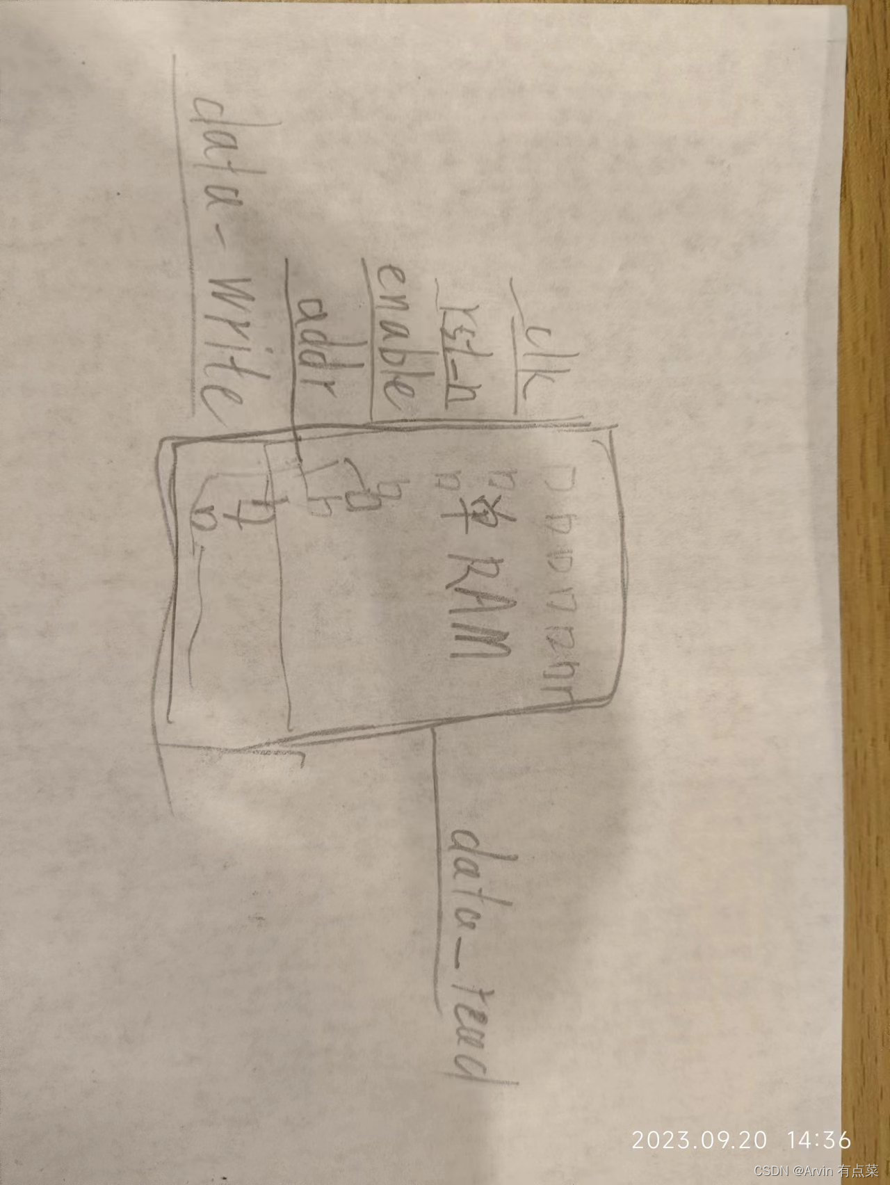
1.3、Verilog实现
module Single_Port_RAM
(
	//system input
	 input 		clk
	,input		rst_n

	//data input
	,input 						enable_wr		//allow the user to read or write the data
														//when enable_wr == 0,it means to write the data from RAM
														//when enable_wr == 1,it means to read the data from RAM
	,input		 	[7:0]		data_write
	,input			[7:0]		address

	//data output
	,output	reg 	[7:0]		data_read
);

//setup RAM which has the width of 8 and depth of 256
localparam 	mem_width = 7;
localparam	mem_depth = 255;
reg	[mem_width:0]		mem	[mem_depth:0];

always @ (posedge clk or negedge rst_n)
begin
	if (!rst_n)
		data_read <= 8'd0;
	else if (!enable_wr)
		mem[address] <= data_write;
	else if (enable_wr)
		data_read <= mem[address];
end
endmodule
1.4、优缺点分析
缺点:同一时刻只能对同一地址进行读操作或者写操作,而不能同时进行;地址处的数据为0时也会读取,可能会发生错误。
优点:简单,不需要协调读写操作;
1.5、TB
验证策略: 先写厚读
写: 在enable为低时,从0地址开始,每次地址加1时加到255,每次给/写一个随机数。查看相应地址中的数据和给/写的输出是否相同,相同则写成功。
读: 在enable为高时,从0地址开始,每次地址加1时加到255,每次读一个数。查看读出的数和相应地址中的数据是否相同,相同则读成功。
二、双端口RAM原理及实现
2.1、原理
参考如上的单端口RAM,双端口RAM在单端口RAM的基础上,将使能信号分为读使能信号和写使能信号,将地址信号分为读地址信号和写地址信号。
2.2 接口

2.3、Verilog实现
module Dual_Port_RAM
(
	//system input
	 input			clk
	,input			rst_n

	//signal of read
	,input						read_en				//when read_en == 1,read the data from mem according to read_addr
	,input			[7:0]		read_addr
	,output	reg 	[7:0]		read_data

	//signal of write
	,input						write_en				//when write_en ==1,write the data to mem according to write_addr
	,input			[7:0]		write_addr
	,input			[7:0]		write_data
);

//setup RAM which has the width of 8 and depth of 256
localparam 	mem_width = 7;
localparam	mem_depth = 255;
reg	[mem_width:0]		mem	[mem_depth:0];
reg	[7:0]		i;

always @ (posedge clk or negedge rst_n)
begin
	if (~rst_n)
		for (i=0;i<=(mem_depth);i=i+1)        //ram初始化
			mem[i] <= 8'd0;
	else if (write_en)
		mem[write_addr] <= write_data;
end

always @ (posedge clk or negedge rst_n)
begin
	if (~rst_n)
		read_data <= 8'd0;		             //数据初始化
	else if (read_en)
		read_data <= mem[read_addr];
	else
		read_data <= read_data;				//when read_en is disabled, read_data maintains the data before
end
endmodule
2.4、优缺点分析
优点:因为地址分为读地址和写地址,所以可以同时对RAM进行读写操作。
1.5、TB
和单端口类似