一,这里实现IIC 读写 EEPROM 的 Verilog 程序,将其打包为 AXI4 IP,从而可以直接将其连入 Zynq 系统。pl_iic_original.v,iic.v 是当前要打包成 AXI4 IP 的新文件。
1,对于 pl_iic_original.v,读写地址 WRITE_READ_ADDR,写数据 WRITE_DATA 是在程序中固定的读开始,写开始,这两个信号是从按键 PL_KEY1,PL_KEY2 获得,读数据直接以 PL 端 LED 来显示。
//----------------------------------------------------------------------------
// Project Name : pl_iic
// Description : EEPROM 24CLC04 Byte Read, Random Write, with IIC serial.
//----------------------------------------------------------------------------
module pl_iic_original(
output SCL, // FPGA output clk signal for 24LC04, 400 KHz (due to now 3.3v Vcc)
inout SDA, // serial input/output address/data
output [3:0] OUT_LED_DATA, // read value from 24LC04, for PL LED to display
input clk, // FPGA input clk, 50 MHz
input rst_n, // FPGA global reset
input PL_KEY1, // press down is 0, means write EEPROM start
input PL_KEY2 // press down is 0, means read EEPROM start
);
key detect
//----------------------------------------------------- key press down confirm
reg [1:0] key_press_down;
reg [1:0] key_press_down_r;
always @(posedge clk, negedge rst_n) begin
if(!rst_n) begin
key_press_down <= 2'b11;
key_press_down_r <= 2'b11;
end
else begin
key_press_down <= {PL_KEY2, PL_KEY1};
key_press_down_r <= key_press_down;
end
end
wire [1:0] key_press_down_conf;
assign key_press_down_conf = key_press_down_r & (~key_press_down);
//------------------------------------------------------ 20ms hysteresis range
reg [19:0] cnt_k;
always @(posedge clk, negedge rst_n) begin
if(!rst_n)
cnt_k <= 20'd0;
else if(key_press_down_conf != 2'd0) // key pressed down found, start count
cnt_k <= 20'd0;
else
cnt_k <= cnt_k + 1'b1;
end
reg [1:0] sampled_key_info;
always @(posedge clk, negedge rst_n) begin
if(!rst_n)
sampled_key_info <= 2'b11;
else if(cnt_k == 20'd99_9999) // 20ms jetter covered, sample the key info
sampled_key_info <= {PL_KEY2, PL_KEY1};
else
sampled_key_info <= 2'b11;
end
wire PL_KEY1_pressed;
wire PL_KEY2_pressed;
assign PL_KEY1_pressed = sampled_key_info[0];
assign PL_KEY2_pressed = sampled_key_info[1];
reg [6:0] cnt;
always @(posedge clk, negedge rst_n) begin
if(!rst_n)
cnt <= 7'd0;
else if(cnt == 7'd124)
cnt <= 7'd0;
else
cnt <= cnt + 1'b1;
end
reg SCL_r;
always @(posedge clk, negedge rst_n) begin
if(!rst_n)
SCL_r <= 1'b0;
else begin
if(cnt == 7'd0)
SCL_r <= 1'b1; // SCL posedge
else if(cnt == 7'd50)
SCL_r <= 1'b0; // SCL negedge
end
end
assign SCL = SCL_r;
// SCL special position label
`define SCL_POSEDGE (cnt == 11'd0)
`define SCL_NEGEDGE (cnt == 11'd50)
`define SCL_HIG_MID (cnt == 11'd25)
`define SCL_LOW_MID (cnt == 11'd87)
wr, rd
// 24LC04 special parameter label
parameter WRITE_CTRL_BYTE = 8'b1010_0000, // select 24LC04 first 256 * 8 bit
READ_CTRL_BYTE = 8'b1010_0001, // select 24LC04 first 256 * 8 bit
WRITE_DATA = 8'b0000_0101, // Write data is 5
WRITE_READ_ADDR = 8'b0001_1110; // Write/Read address is 0x1E
reg SDA_r;
reg SDA_en;
assign SDA = SDA_en ? SDA_r : 1'bz; // SDA_en == 1, means SDA as output, it will get SDA_r
// SDA_en == 0, means SDA as input, it drived by the 24LC04, so high-z SDA_r out line
reg [3:0] OUT_LED_DATA_reg;
assign OUT_LED_DATA = OUT_LED_DATA_reg;
parameter IDLE = 5'd0,
// Write state (BYTE WRITE, refer to 24LC04 datasheet)
START_W = 5'd1,
SEND_CTRL_BYTE_W = 5'd2,
RECEIVE_ACK_1_W = 5'd3,
SEND_ADDR_BYTE_W = 5'd4,
RECEIVE_ACK_2_W = 5'd5,
SEND_DATA_BYTE_W = 5'd6,
RECEIVE_ACK_3_W = 5'd7,
STOP_W = 5'd8,
// Read state (RANDOM READ, refer to 24LC04 datasheet)
START_R_1 = 5'd9,
SEND_CTRL_BYTE_1_R = 5'd10,
RECEIVE_ACK_1_R = 5'd11,
SEND_ADDR_BYTE_R = 5'd12,
RECEIVE_ACK_2_R = 5'd13,
START_R_2 = 5'd14,
SEND_CTRL_BYTE_2_R = 5'd15,
RECEIVE_ACK_3_R = 5'd16,
RECEIVE_DATA_R = 5'd17,
STOP_R = 5'd18;
reg [4:0] state;
reg [3:0] write_byte_cnt;
reg [7:0] write_byte_reg;
always @(posedge clk, negedge rst_n) begin
if(!rst_n) begin
state <= IDLE;
write_byte_cnt <= 4'd0;
write_byte_reg <= 8'd0;
OUT_LED_DATA_reg <= 4'b1111; // LED all off
SDA_en <= 1'b0;
end
else begin
case(state)
IDLE: begin
SDA_en <= 1'b1;
SDA_r <= 1'b1;
if(PL_KEY1_pressed == 1'b0) begin
state <= START_W;
end
else if(PL_KEY2_pressed == 1'b0)
state <= START_R_1;
else
state <= IDLE;
end
//------------------------------------------ BYTE WRITE FSM START
START_W: begin
if(`SCL_HIG_MID) begin
SDA_r <= 1'b0;
write_byte_cnt <= 4'd0;
write_byte_reg <= WRITE_CTRL_BYTE;
state <= SEND_CTRL_BYTE_W;
end
else
state <= START_W;
end
SEND_CTRL_BYTE_W: begin
if(`SCL_LOW_MID) begin
case(write_byte_cnt)
0: SDA_r <= write_byte_reg[7];
1: SDA_r <= write_byte_reg[6];
2: SDA_r <= write_byte_reg[5];
3: SDA_r <= write_byte_reg[4];
4: SDA_r <= write_byte_reg[3];
5: SDA_r <= write_byte_reg[2];
6: SDA_r <= write_byte_reg[1];
7: SDA_r <= write_byte_reg[0];
default: ;
endcase
write_byte_cnt <= write_byte_cnt + 1'b1;
if(write_byte_cnt == 4'd8) begin
write_byte_cnt <= 4'd0;
SDA_en <= 1'b0; // wait the 24LC04 to reponse ACK, so SDA as input
state <= RECEIVE_ACK_1_W;
end
else
state <= SEND_CTRL_BYTE_W;
end
end
RECEIVE_ACK_1_W: begin
if(`SCL_NEGEDGE) begin
write_byte_reg <= WRITE_READ_ADDR;
SDA_en <= 1'b1;
state <= SEND_ADDR_BYTE_W;
end
else
state <= RECEIVE_ACK_1_W;
end
SEND_ADDR_BYTE_W: begin
if(`SCL_LOW_MID) begin
case(write_byte_cnt)
0: SDA_r <= write_byte_reg[7];
1: SDA_r <= write_byte_reg[6];
2: SDA_r <= write_byte_reg[5];
3: SDA_r <= write_byte_reg[4];
4: SDA_r <= write_byte_reg[3];
5: SDA_r <= write_byte_reg[2];
6: SDA_r <= write_byte_reg[1];
7: SDA_r <= write_byte_reg[0];
default: ;
endcase
write_byte_cnt <= write_byte_cnt + 1'b1;
if(write_byte_cnt == 4'd8) begin
write_byte_cnt <= 4'd0;
SDA_en <= 1'b0; // wait the 24LC04 to reponse ACK, so SDA as input
state <= RECEIVE_ACK_2_W;
end
else
state <= SEND_ADDR_BYTE_W;
end
end
RECEIVE_ACK_2_W: begin
if(`SCL_NEGEDGE) begin
write_byte_reg <= WRITE_DATA;
SDA_en <= 1'b1;
state <= SEND_DATA_BYTE_W;
end
else
state <= RECEIVE_ACK_2_W;
end
SEND_DATA_BYTE_W: begin
if(`SCL_LOW_MID) begin
case(write_byte_cnt)
0: SDA_r <= write_byte_reg[7];
1: SDA_r <= write_byte_reg[6];
2: SDA_r <= write_byte_reg[5];
3: SDA_r <= write_byte_reg[4];
4: SDA_r <= write_byte_reg[3];
5: SDA_r <= write_byte_reg[2];
6: SDA_r <= write_byte_reg[1];
7: SDA_r <= write_byte_reg[0];
default: ;
endcase
write_byte_cnt <= write_byte_cnt + 1'b1;
if(write_byte_cnt == 4'd8) begin
write_byte_cnt <= 4'd0;
SDA_en <= 1'b0; // wait the 24LC04 to reponse ACK, so SDA as input
state <= RECEIVE_ACK_3_W;
end
else
state <= SEND_DATA_BYTE_W;
end
end
RECEIVE_ACK_3_W: begin
if(`SCL_NEGEDGE) begin
SDA_en <= 1'b1;
state <= STOP_W;
end
else
state <= RECEIVE_ACK_3_W;
end
STOP_W: begin
if(`SCL_LOW_MID)
SDA_r <= 1'b0;
else if(`SCL_HIG_MID) begin
SDA_r <= 1'b1;
OUT_LED_DATA_reg <= 4'b0000; // when write succeed, all LED turn on
state <= IDLE;
end
end
//------------------------------------------ BYTE WRITE FSM END
//------------------------------------------ RANDOM READ FSM START
START_R_1: begin
if(`SCL_HIG_MID) begin
SDA_r <= 1'b0;
write_byte_cnt <= 4'd0;
write_byte_reg <= WRITE_CTRL_BYTE;
state <= SEND_CTRL_BYTE_1_R;
end
else
state <= START_R_1;
end
SEND_CTRL_BYTE_1_R: begin
if(`SCL_LOW_MID) begin
case(write_byte_cnt)
0: SDA_r <= write_byte_reg[7];
1: SDA_r <= write_byte_reg[6];
2: SDA_r <= write_byte_reg[5];
3: SDA_r <= write_byte_reg[4];
4: SDA_r <= write_byte_reg[3];
5: SDA_r <= write_byte_reg[2];
6: SDA_r <= write_byte_reg[1];
7: SDA_r <= write_byte_reg[0];
default: ;
endcase
write_byte_cnt <= write_byte_cnt + 1'b1;
if(write_byte_cnt == 4'd8) begin
write_byte_cnt <= 4'd0;
SDA_en <= 1'b0; // wait the 24LC04 to reponse ACK, so SDA as input
state <= RECEIVE_ACK_1_R;
end
else
state <= SEND_CTRL_BYTE_1_R;
end
end
RECEIVE_ACK_1_R: begin
if(`SCL_NEGEDGE) begin
SDA_en <= 1'b1;
write_byte_reg <= WRITE_READ_ADDR;
state <= SEND_ADDR_BYTE_R;
end
else
state <= RECEIVE_ACK_1_R;
end
SEND_ADDR_BYTE_R: begin
if(`SCL_LOW_MID) begin
case(write_byte_cnt)
0: SDA_r <= write_byte_reg[7];
1: SDA_r <= write_byte_reg[6];
2: SDA_r <= write_byte_reg[5];
3: SDA_r <= write_byte_reg[4];
4: SDA_r <= write_byte_reg[3];
5: SDA_r <= write_byte_reg[2];
6: SDA_r <= write_byte_reg[1];
7: SDA_r <= write_byte_reg[0];
default: ;
endcase
write_byte_cnt <= write_byte_cnt + 1'b1;
if(write_byte_cnt == 4'd8) begin
write_byte_cnt <= 4'd0;
SDA_en <= 1'b0; // wait the 24LC04 to reponse ACK, so SDA as input
state <= RECEIVE_ACK_2_R;
end
else
state <= SEND_ADDR_BYTE_R;
end
end
RECEIVE_ACK_2_R: begin
if(`SCL_NEGEDGE) begin
SDA_en <= 1'b1;
SDA_r <= 1'b1; // for START_R_2
state <= START_R_2;
end
else
state <= RECEIVE_ACK_2_R;
end
START_R_2: begin
if(`SCL_HIG_MID) begin
SDA_r <= 1'b0;
write_byte_cnt <= 4'd0;
write_byte_reg <= READ_CTRL_BYTE;
state <= SEND_CTRL_BYTE_2_R;
end
else
state <= START_R_2;
end
SEND_CTRL_BYTE_2_R: begin
if(`SCL_LOW_MID) begin
case(write_byte_cnt)
0: SDA_r <= write_byte_reg[7];
1: SDA_r <= write_byte_reg[6];
2: SDA_r <= write_byte_reg[5];
3: SDA_r <= write_byte_reg[4];
4: SDA_r <= write_byte_reg[3];
5: SDA_r <= write_byte_reg[2];
6: SDA_r <= write_byte_reg[1];
7: SDA_r <= write_byte_reg[0];
default: ;
endcase
write_byte_cnt <= write_byte_cnt + 1'b1;
if(write_byte_cnt == 4'd8) begin
write_byte_cnt <= 4'd0;
SDA_en <= 1'b0; // wait the 24LC04 to reponse Read Data, so SDA as input
state <= RECEIVE_ACK_3_R;
end
else
state <= SEND_CTRL_BYTE_2_R;
end
end
RECEIVE_ACK_3_R: begin
if(`SCL_NEGEDGE) begin
state <= RECEIVE_DATA_R;
end
else
state <= RECEIVE_ACK_3_R;
end
RECEIVE_DATA_R: begin
if(`SCL_HIG_MID) begin
case(write_byte_cnt)
0: write_byte_reg[7] <= SDA;
1: write_byte_reg[6] <= SDA;
2: write_byte_reg[5] <= SDA;
3: write_byte_reg[4] <= SDA;
4: write_byte_reg[3] <= SDA;
5: write_byte_reg[2] <= SDA;
6: write_byte_reg[1] <= SDA;
7: write_byte_reg[0] <= SDA;
default: ;
endcase
write_byte_cnt <= write_byte_cnt + 1'b1;
if(write_byte_cnt == 4'd8) begin
write_byte_cnt <= 4'd0;
SDA_en <= 1'b1; // 24LC04 response data over, so make SDA as output
state <= STOP_R;
end
end
else
state <= RECEIVE_DATA_R;
end
STOP_R: begin
if(`SCL_LOW_MID)
SDA_r <= 1'b0;
else if(`SCL_HIG_MID) begin
SDA_r <= 1'b1;
OUT_LED_DATA_reg <= write_byte_reg[3:0]; // when read done, LED display the data
state <= IDLE;
end
end
endcase
end
end
endmodule2,iic.v,读写地址 WRITE_READ_ADDR,写数据 WRITE_DATA,写开始信号 WRITE_START,读开始信号 READ_START 都是从 AXI 总线获得,在 SDK 软件中配置。而读数据 READ_DATA,读完成 READ_DONE,写完成 WRITE_DONE 送到 AXI 总线,在 SDK 软件中检测。
//----------------------------------------------------------------------------
// Project Name : pl_iic
// Description : EEPROM 24CLC04 Byte Read, Random Write, with IIC serial.
//----------------------------------------------------------------------------
module iic(
output SCL, //FPGA output clk signal for 24LC04, 400 KHz (3.3v Vcc)
inout SDA, // input/output serial address/data
// data send to AXI bus
output [7:0] READ_DATA,
output READ_DONE, // when read done, pull up
output WRITE_DONE, // when write done, pull up
// data get from AXI bus
input [7:0] WRITE_READ_ADDR,
input [7:0] WRITE_DATA,
input WRITE_START, // when PL KEY1 pressed, pull up
input READ_START, // when PL KEY2 pressed, pull up
input clk, // Fabric clk, 50 MHz
input rst_n // Async reset from Zynq System Reset module, low level active
);
reg [6:0] cnt;
always @(posedge clk, negedge rst_n) begin
if(!rst_n)
cnt <= 7'd0;
else if(cnt == 7'd124)
cnt <= 7'd0;
else
cnt <= cnt + 1'b1;
end
reg SCL_r;
always @(posedge clk, negedge rst_n) begin
if(!rst_n)
SCL_r <= 1'b0;
else begin
if(cnt == 7'd0)
SCL_r <= 1'b1; // SCL posedge
else if(cnt == 7'd50)
SCL_r <= 1'b0; // SCL negedge
end
end
assign SCL = SCL_r;
// SCL special position label
`define SCL_POSEDGE (cnt == 11'd0)
`define SCL_NEGEDGE (cnt == 11'd50)
`define SCL_HIG_MID (cnt == 11'd25)
`define SCL_LOW_MID (cnt == 11'd87)
//----------------------------------------------------------------------------
// 24LC04 special parameter label
parameter WRITE_CTRL_BYTE = 8'b1010_0000, // select 24LC04 first 256 * 8 bit
READ_CTRL_BYTE = 8'b1010_0001; // select 24LC04 first 256 * 8 bit
reg SDA_r;
reg SDA_en;
assign SDA = SDA_en ? SDA_r : 1'bz; // SDA_en == 1, means SDA as output, it will get SDA_r
// SDA_en == 0, means SDA as input, it drived by the 24LC04, so high-z SDA_r out line
reg [7:0] READ_DATA_reg;
assign READ_DATA = READ_DATA_reg;
reg READ_DONE_reg;
assign READ_DONE = READ_DONE_reg;
reg WRITE_DONE_reg;
assign WRITE_DONE = WRITE_DONE_reg;
parameter IDLE = 5'd0,
// Write state (BYTE WRITE, refer to 24LC04 datasheet)
START_W = 5'd1,
SEND_CTRL_BYTE_W = 5'd2,
RECEIVE_ACK_1_W = 5'd3,
SEND_ADDR_BYTE_W = 5'd4,
RECEIVE_ACK_2_W = 5'd5,
SEND_DATA_BYTE_W = 5'd6,
RECEIVE_ACK_3_W = 5'd7,
STOP_W = 5'd8,
// Read state (RANDOM READ, refer to 24LC04 datasheet)
START_R_1 = 5'd9,
SEND_CTRL_BYTE_1_R = 5'd10,
RECEIVE_ACK_1_R = 5'd11,
SEND_ADDR_BYTE_R = 5'd12,
RECEIVE_ACK_2_R = 5'd13,
START_R_2 = 5'd14,
SEND_CTRL_BYTE_2_R = 5'd15,
RECEIVE_ACK_3_R = 5'd16,
RECEIVE_DATA_R = 5'd17,
STOP_R = 5'd18;
reg [4:0] state;
reg [3:0] write_byte_cnt;
reg [7:0] write_byte_reg;
always @(posedge clk, negedge rst_n) begin
if(!rst_n) begin
state <= IDLE;
write_byte_cnt <= 4'd0;
write_byte_reg <= 8'd0;
READ_DATA_reg <= 8'd0;
READ_DONE_reg <= 1'b0;
WRITE_DONE_reg <= 1'b0;
SDA_en <= 1'b0;
end
else begin
case(state)
IDLE: begin
SDA_en <= 1'b1;
SDA_r <= 1'b1;
if(WRITE_START) begin
WRITE_DONE_reg <= 1'b0;
state <= START_W;
end
else if(READ_START) begin
READ_DONE_reg <= 1'b0;
state <= START_R_1;
end
else
state <= IDLE;
end
//------------------------------------------ BYTE WRITE FSM START
START_W: begin
if(`SCL_HIG_MID) begin
SDA_r <= 1'b0;
write_byte_cnt <= 4'd0;
write_byte_reg <= WRITE_CTRL_BYTE;
state <= SEND_CTRL_BYTE_W;
end
else
state <= START_W;
end
SEND_CTRL_BYTE_W: begin
if(`SCL_LOW_MID) begin
case(write_byte_cnt)
0: SDA_r <= write_byte_reg[7];
1: SDA_r <= write_byte_reg[6];
2: SDA_r <= write_byte_reg[5];
3: SDA_r <= write_byte_reg[4];
4: SDA_r <= write_byte_reg[3];
5: SDA_r <= write_byte_reg[2];
6: SDA_r <= write_byte_reg[1];
7: SDA_r <= write_byte_reg[0];
default: ;
endcase
write_byte_cnt <= write_byte_cnt + 1'b1;
if(write_byte_cnt == 4'd8) begin
write_byte_cnt <= 4'd0;
SDA_en <= 1'b0; // wait the 24LC04 to reponse ACK, so SDA as input
state <= RECEIVE_ACK_1_W;
end
else
state <= SEND_CTRL_BYTE_W;
end
end
RECEIVE_ACK_1_W: begin
if(`SCL_NEGEDGE) begin
write_byte_reg <= WRITE_READ_ADDR;
SDA_en <= 1'b1;
state <= SEND_ADDR_BYTE_W;
end
else
state <= RECEIVE_ACK_1_W;
end
SEND_ADDR_BYTE_W: begin
if(`SCL_LOW_MID) begin
case(write_byte_cnt)
0: SDA_r <= write_byte_reg[7];
1: SDA_r <= write_byte_reg[6];
2: SDA_r <= write_byte_reg[5];
3: SDA_r <= write_byte_reg[4];
4: SDA_r <= write_byte_reg[3];
5: SDA_r <= write_byte_reg[2];
6: SDA_r <= write_byte_reg[1];
7: SDA_r <= write_byte_reg[0];
default: ;
endcase
write_byte_cnt <= write_byte_cnt + 1'b1;
if(write_byte_cnt == 4'd8) begin
write_byte_cnt <= 4'd0;
SDA_en <= 1'b0; // wait the 24LC04 to reponse ACK, so SDA as input
state <= RECEIVE_ACK_2_W;
end
else
state <= SEND_ADDR_BYTE_W;
end
end
RECEIVE_ACK_2_W: begin
if(`SCL_NEGEDGE) begin
write_byte_reg <= WRITE_DATA;
SDA_en <= 1'b1;
state <= SEND_DATA_BYTE_W;
end
else
state <= RECEIVE_ACK_2_W;
end
SEND_DATA_BYTE_W: begin
if(`SCL_LOW_MID) begin
case(write_byte_cnt)
0: SDA_r <= write_byte_reg[7];
1: SDA_r <= write_byte_reg[6];
2: SDA_r <= write_byte_reg[5];
3: SDA_r <= write_byte_reg[4];
4: SDA_r <= write_byte_reg[3];
5: SDA_r <= write_byte_reg[2];
6: SDA_r <= write_byte_reg[1];
7: SDA_r <= write_byte_reg[0];
default: ;
endcase
write_byte_cnt <= write_byte_cnt + 1'b1;
if(write_byte_cnt == 4'd8) begin
write_byte_cnt <= 4'd0;
SDA_en <= 1'b0; // wait the 24LC04 to reponse ACK, so SDA as input
state <= RECEIVE_ACK_3_W;
end
else
state <= SEND_DATA_BYTE_W;
end
end
RECEIVE_ACK_3_W: begin
if(`SCL_NEGEDGE) begin
SDA_en <= 1'b1;
state <= STOP_W;
end
else
state <= RECEIVE_ACK_3_W;
end
STOP_W: begin
if(`SCL_LOW_MID)
SDA_r <= 1'b0;
else if(`SCL_HIG_MID) begin
SDA_r <= 1'b1;
WRITE_DONE_reg <= 1'b1;
state <= IDLE;
end
end
//------------------------------------------ BYTE WRITE FSM END
//------------------------------------------ RANDOM READ FSM START
START_R_1: begin
if(`SCL_HIG_MID) begin
SDA_r <= 1'b0;
write_byte_cnt <= 4'd0;
write_byte_reg <= WRITE_CTRL_BYTE;
state <= SEND_CTRL_BYTE_1_R;
end
else
state <= START_R_1;
end
SEND_CTRL_BYTE_1_R: begin
if(`SCL_LOW_MID) begin
case(write_byte_cnt)
0: SDA_r <= write_byte_reg[7];
1: SDA_r <= write_byte_reg[6];
2: SDA_r <= write_byte_reg[5];
3: SDA_r <= write_byte_reg[4];
4: SDA_r <= write_byte_reg[3];
5: SDA_r <= write_byte_reg[2];
6: SDA_r <= write_byte_reg[1];
7: SDA_r <= write_byte_reg[0];
default: ;
endcase
write_byte_cnt <= write_byte_cnt + 1'b1;
if(write_byte_cnt == 4'd8) begin
write_byte_cnt <= 4'd0;
SDA_en <= 1'b0; // wait the 24LC04 to reponse ACK, so SDA as input
state <= RECEIVE_ACK_1_R;
end
else
state <= SEND_CTRL_BYTE_1_R;
end
end
RECEIVE_ACK_1_R: begin
if(`SCL_NEGEDGE) begin
SDA_en <= 1'b1;
write_byte_reg <= WRITE_READ_ADDR;
state <= SEND_ADDR_BYTE_R;
end
else
state <= RECEIVE_ACK_1_R;
end
SEND_ADDR_BYTE_R: begin
if(`SCL_LOW_MID) begin
case(write_byte_cnt)
0: SDA_r <= write_byte_reg[7];
1: SDA_r <= write_byte_reg[6];
2: SDA_r <= write_byte_reg[5];
3: SDA_r <= write_byte_reg[4];
4: SDA_r <= write_byte_reg[3];
5: SDA_r <= write_byte_reg[2];
6: SDA_r <= write_byte_reg[1];
7: SDA_r <= write_byte_reg[0];
default: ;
endcase
write_byte_cnt <= write_byte_cnt + 1'b1;
if(write_byte_cnt == 4'd8) begin
write_byte_cnt <= 4'd0;
SDA_en <= 1'b0; // wait the 24LC04 to reponse ACK, so SDA as input
state <= RECEIVE_ACK_2_R;
end
else
state <= SEND_ADDR_BYTE_R;
end
end
RECEIVE_ACK_2_R: begin
if(`SCL_NEGEDGE) begin
SDA_en <= 1'b1;
SDA_r <= 1'b1; // for START_R_2
state <= START_R_2;
end
else
state <= RECEIVE_ACK_2_R;
end
START_R_2: begin
if(`SCL_HIG_MID) begin
SDA_r <= 1'b0;
write_byte_cnt <= 4'd0;
write_byte_reg <= READ_CTRL_BYTE;
state <= SEND_CTRL_BYTE_2_R;
end
else
state <= START_R_2;
end
SEND_CTRL_BYTE_2_R: begin
if(`SCL_LOW_MID) begin
case(write_byte_cnt)
0: SDA_r <= write_byte_reg[7];
1: SDA_r <= write_byte_reg[6];
2: SDA_r <= write_byte_reg[5];
3: SDA_r <= write_byte_reg[4];
4: SDA_r <= write_byte_reg[3];
5: SDA_r <= write_byte_reg[2];
6: SDA_r <= write_byte_reg[1];
7: SDA_r <= write_byte_reg[0];
default: ;
endcase
write_byte_cnt <= write_byte_cnt + 1'b1;
if(write_byte_cnt == 4'd8) begin
write_byte_cnt <= 4'd0;
SDA_en <= 1'b0; // wait the 24LC04 to reponse Read Data, so SDA as input
state <= RECEIVE_ACK_3_R;
end
else
state <= SEND_CTRL_BYTE_2_R;
end
end
RECEIVE_ACK_3_R: begin
if(`SCL_NEGEDGE) begin
state <= RECEIVE_DATA_R;
end
else
state <= RECEIVE_ACK_3_R;
end
RECEIVE_DATA_R: begin
if(`SCL_HIG_MID) begin
case(write_byte_cnt)
0: write_byte_reg[7] <= SDA;
1: write_byte_reg[6] <= SDA;
2: write_byte_reg[5] <= SDA;
3: write_byte_reg[4] <= SDA;
4: write_byte_reg[3] <= SDA;
5: write_byte_reg[2] <= SDA;
6: write_byte_reg[1] <= SDA;
7: write_byte_reg[0] <= SDA;
default: ;
endcase
write_byte_cnt <= write_byte_cnt + 1'b1;
if(write_byte_cnt == 4'd8) begin
write_byte_cnt <= 4'd0;
SDA_en <= 1'b1; // 24LC04 response data over, so make SDA as output
state <= STOP_R;
end
end
else
state <= RECEIVE_DATA_R;
end
STOP_R: begin
if(`SCL_LOW_MID)
SDA_r <= 1'b0;
else if(`SCL_HIG_MID) begin
SDA_r <= 1'b1;
READ_DATA_reg <= write_byte_reg;
READ_DONE_reg <= 1'b1;
state <= IDLE;
end
end
endcase
end
end
endmodule二,新建AXI4 IP
1,打开vivado,选择菜单栏 Tools > Create and Package IP

2,其中 Package a new IP for the Vivado IP Catalog 就是我们自定义 IP 时采用的两种方式,即打包工程或打包文件夹。其中Create a new AXI4Peripheral 就是创建 AXI4 外设 IP。点击 Next。

3,选择 Create a new AXI4 peripheral,点击 Next

4,填写要打包的AXI 外设 IP 的信息。这里修改了 Name 名称,Description 描述,和打包存储的路径 IP location。可以自行定义这些信息,点击 Next。

5,iic.v 的模块头, AXI IP 有 7 个寄存器要放在 AXI 总线上,所以如下的寄存器个数填为 7,其它选项保持默认,点击 Next。

Summary 窗口,选项保持默认值,点击 Finish 完成。

6,下点击左侧边栏 Project Manager 底下的 IP Catalog,打开 IP 列表窗口。在 IP Catalog 窗口,已经有了我们自定义的 AXI IP;

三,修改IP代码
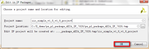
1,右键单击 iic_simple_v1.0 选择 Edit in IP Packager 选项;

2,如下弹窗点击 OK,将打开一个临时的 IP packager 工程
在 Source 窗口,双击打开 iic_simple_v1_0 文件进行编辑,

3,增加 IIC 的端口列表,再增加例化列表,所示:

4,在 Source 窗口,双击打开 iic_simple_v1_0_S00_AXI_inst 文件进行编辑,增加端口列表。

5,再将 7 个 register 中的后三个改为 wire 型存储从 AXI 总线上读取的值,不对其进行设置

6,然后例化 IIC 模块,如下,其中,slv_reg0,slv_reg1,slv_reg2,slv_reg3 分别在 SDK 软件中设置读写地址,写数据,写开始,读开始信号,这些数据设置好之后送往 AXI 总线。slv_reg4,
slv_reg5,slv_reg6 作为读数据,读完成,写完成的暂存位置,这些数据从 AXI 总线上获得,在SDK 软件中进行处理。
