After the understanding and familiarity of the first two parts, the understanding of SRAM is basically clear.
You can use the knowledge you have learned here, and you can establish your own methodology and process for the generation and selection of SRAM. In this chapter, the author shares some insights and brainstorms and discusses this automated process.

SRAM generation method
Based on different processes and FAB, there will be a corresponding memory team to build memory array and peripheral for the specified process. The construction here refers to the construction of some basic components, which are then packaged and delivered to users in the form of automated commands, which is convenient for users to perform different configurations and selections.
The kits provided by different SRAM vendors are often different, some can support GUI and batch, and some support batch. In comparison, batch must be supported, otherwise this kind of work cannot be carried out in batches under large-scale projects. Here we take the T family as an example, using batch mode to generate SRAM
> tsn7_1prf.exe -NonTsmcName -file $CFG_FILE
Each SRAM has its own default name, but for the convenience of data management, users usually need to use their own name for planning, so when using T’s mem-gen, it is recommended that you use your own $CFG_FILE for name definition. Of course, the $CFG_FILE here needs to specify the specific bit width, bit depth and column MUX information of the SRAM. A simple example is as follows
 )
)
T's command line also supports some other options, including but not limited to
- SRAM datasheet: Contains various timing, power consumption and physical information of SRAM
- Generation options for various views
- verilog simulation model
- DFT view
- timing view
- Masis view
- SPICE view
- GDS view
- LEF view
- VOLTUS view
- Selection of different configurations (in view of the different types of memory, not every configuration can generate the corresponding memory, users need to check the memgen log)
- DualRail: Use different rails for VDD/VDDM
- ULVT/SVT: the choice of peripheral std-cell VT,
- BIST: Control whether to support MBIST mode
- bit-wise: whether to support bit write operation
- etc…
All configurable interfaces can be configured in batch mode. The advantage of this is that it can support users to realize automation when selecting and generating large-area SRAMs.
Similar SNPS will provide batch and GUI interface in mem-gen. GUI operation is relatively convenient, but in batch production, it is still necessary to use batch to improve production efficiency
 )
)
SRAM selection dimensions in actual projects
With the above explanations and the support of tools, users can basically start to generate SRAM. The above information and resources are ultimately tools to support actual projects. The comparison, matching, and selection of different SRAMs are the actual projects that can really work.
In today's large-scale chips, the area used by SRAM can even account for nearly half of the area of the entire project, so the selection of SRAM needs to be considered from the following aspects
-
Selection of SRAM vendor based on process
- Channel 1: Usually when FAB provides the process, it will also provide SRAM vendor recommendations. Generally speaking, FAB’s own SRAM is generally free (it should be covered by TO fees), such as T or S. Provide SRAM products with their own corresponding process
- Channel 2: Some third-party SRAM vendors have established a solid commercial contract with FAB, and FAB will also share it with users, allowing users to choose by themselves. Users only need a small amount of royalties when tape-out .
- Channel 3: For a certain process, some commercial customers have specially developed SRAM, and can achieve a better PPA than the original FAB, such as S, A, etc. At this time, when users use it, they need to use it like Purchasing IP is the same as paying extra. If users really rely on a certain PPA, they can consider spending this money.
-
Consideration of Rail: Since this involves the rail design of the entire chip, it must be considered clearly at the early stage, and the project usually adopts a unified strategy. The current SRAM supports SD/DSLP design without the loss of peripheral isolate logic, but the internal processing of SRAM must have the cost of isolate. Based on the project's balance between power consumption and performance, it is very necessary to select the rail mode at the initial stage.
-
DFT correlation of STAM:
- BIST: Since there are peripheral std-cells in SRAM, the DFT function of this MBIST can support the fault location of such std-cells. The cost is due to the sharp increase of input pins, which may be a new challenge for APR. Usually, in order to save winding resources, these peripheral std-cell MBIST tests will be skipped, and MBIST tests will be performed on the entire memory (including memory array) directly.

- BISR: In order to achieve the yield rate, BISR is sometimes needed, especially the column redundancy bit. Through the data provided by FAB, 1 bit redundancy can usually be repaired, inspected and doubled , and the cost performance is still very high.
- All SRAM DFT-related parts require additional STD-cell support. This type of area is usually about 5% to 10% of the memory area. For large-scale chips, the impact of this part needs to be comprehensive when designing the architecture and evaluating the area. to consider
- BIST: Since there are peripheral std-cells in SRAM, the DFT function of this MBIST can support the fault location of such std-cells. The cost is due to the sharp increase of input pins, which may be a new challenge for APR. Usually, in order to save winding resources, these peripheral std-cell MBIST tests will be skipped, and MBIST tests will be performed on the entire memory (including memory array) directly.
-
Shape: Due to the existence of too much memory (or memory array), the memory shape has a relatively large impact on the floorplan and pin access of APR. For a specific example, see: Let’s do a decoration layout to realize the second step – Floorplan . Here are a few points to note:
- Do not set the column mux too large for speed reasons. Causes memory to be too flat
- Do not create a memory that is too small in size, as it may cause the conventional pg strap not to fall directly on the memory, reduce power connection performance, and so on.
-
Timing: Here we focus on timing. Due to the wide distribution of memory, when the project is very large, the timing problem of memory will become the performance bottleneck of some core components, such as: L1/L2 etc. Therefore, when selecting memory, here are a few special attentions elements
-
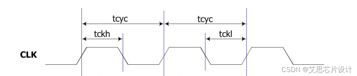
Tcycle: Minimum CLK cycle time CLK^ CLK^. This parameter describes the minimum period (highest frequency) that the memory can support, which must be higher than the frequency planned by the project. In addition, since this parameter is also a lookup table for clock input transition, usually the first version of clock-transition will It is defined as about 50ps, so it is suggested here that when selecting memory, Tcycle needs to have a margin of 20% more than the project requirements. If the main frequency of the project is 1G, then it is required that the Tcycle time of the SRAM cannot exceed 0.8ns under the condition of ssg
-
Tckh/Tckl Minimum CLK Pulse High/Low. Usually each is about half of the Tcycle. It is important to note here that for a clock network with too many stages (latency is too long), the clock inverter must be used first to build a clock tree, so as to control the duty cycle of the leaf (memory clock pin) Ratio, that is, try to satisfy: Tckh/Tckl
-
Tcd/Tacc: CLK to valid Q (data output). This is to describe the time from memory to Q output, which has a great influence on the datapath of from-memory.
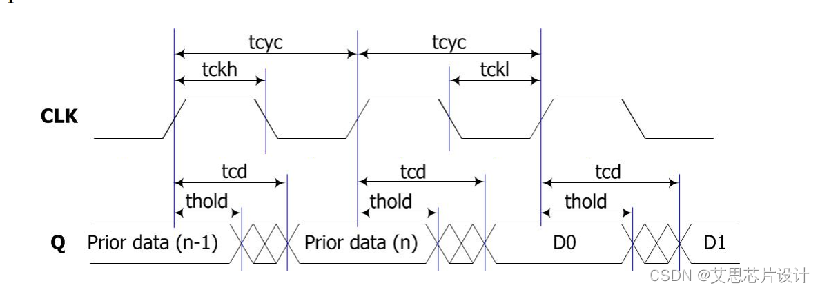
Since the size of the memory is usually relatively large, the access time is usually 200ps~up, so for a timing path, this may be the maximum loss of data on a path. You can see that if you pass it, you can reduce Tqd and Tcd or increase it
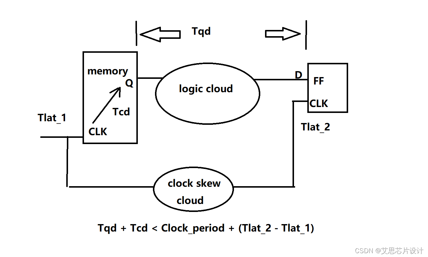
. Useful skew (Tlat_2 - Tlat_1), can improve the performance of the chip.
Usually for Tcd, it is advisable not to exceed 60% of the entire period
-
-
Power consumption: The power consumption of different types of memory is also different. At this time, the ratio of ULVT and LVT of the peripheral of the memory will make a significant difference in leakage. When selecting the type, it is necessary to distinguish the impact of these two types on the timing Influence, so as to adopt the appropriate type.
Simple process of SRAM generation in actual projects
Through the understanding of the various attributes of memory, the following simple process can be used here for the generation and selection process
- Determine common memory requirements for rail and DFT
- Clarify the bit depth and bit width requirements of the memory. If it is too large, it needs to be split manually or automatically based on the rules defined by the front and back ends.
- Batch generation of memory that meets the above requirements: bit width, bit depth, column MUX and LVT/ULVT and other configurations are different, and the results are not the same. Here, it is necessary to traverse all possibilities and increase the selection range
- Perform timing performance analysis on all memory. The memory that can be used only needs to meet the Tcd and Tcycle margins described above at the same time.
- If there is a memory that meets the timing requirements, re-select the power consumption and aspect ratio, and select a memory with low power consumption and reasonable aspect ratio for delivery; if there is no memory that meets the timing requirements, re-split (usually the The bit is cut in half, the timing will be easier to meet), and then repeat steps 3~5 until a suitable memory is selected.
Main points:
- The amount of generated data in memory is huge, and scripted generation mode must be used, for example: excel-> perl -> memgen batch run -> analyze datasheet -> release suitable memory.
- In the initial stage of model selection, you can only look at the datasheet, and other views can not be generated first, which can improve speed and reduce disk usage.
- The CM should not be too large to meet the timing. It can be properly split to make the shape of the memory more reasonable.
- By default, LVT is used for memory peripheral planning. If the ECO stage has timing obstacles, you can consider switching to ULVT for local timing pushing. You can sacrifice part of the leakage in exchange for performance and save iteration cycles.
- The corresponding physical memory of the same logic memory should be selected with the same specifications as much as possible, so that it will be easy to handle during floorplan layout, reduce channels, and improve utilization.
Vocabulary in this chapter
| vocabulary | explain |
|---|---|
| Tcycle | Minimum period supported by memory (highest frequency) |
| Tcd/Tacc | Memory access time CLK->Q |
[Knock on the blackboard to draw key points]

Through the study of three articles, I have a basic understanding and understanding of the structure, principle, characteristic parameters, batch generation and project selection of memory. I hope this series of articles can bring you inspiration and inspiration, and you can be better in the project Understand and apply memory properly, bringing more efficient benefits and PPA to the project.
References
TSMC TSMC N7 SRAM Compiler Databook
Synopsys Embed-It! Integrator User Manual