NVIDIA GPU Turing架构简述
本文摘抄自Turing官方白皮书:https://www.nvidia.com/content/dam/en-zz/Solutions/design-visualization/technologies/turing-architecture/NVIDIA-Turing-Architecture-Whitepaper.pdf
SM
Turing的流式多处理器(SM)和Volta的架构相同,都是7.x。
The Turing Streaming Multiprocessor (SM) is based on the same major architecture (7.x) as Volta, and provides similar improvements over Pascal.
每个SM包含4和线程束调度单元,每个调度单元处理一个线程束组,并有一组专用的算术指令单元。
Each Turing SM includes 4 warp-scheduler units.Each scheduler handles a static set of warps and issues to a dedicated set of arithmetic instruction units.
指令在两个周期内执行,调度器可以在每个周期发出独立的指令。而核心数学运算相关指令如FMA需要4个周期的延迟,与Volta相同,但比Pascal的六个周期要短。
Instructions are performed over two cycles, and the schedulers can issue independent instructions every cycle. Dependent instruction issue latency for core FMA math operations is four clock cycles, like Volta, compared to six cycles on Pascal.
与Volta架构类似,Turing提供了64个fp32核心,64个int32核心和8个改进的混合精度Tensor Cores核心。这使得fp32和int32的操作可以同时执行。但Turing仅提供2个fp64核心,因此双精度的计算吞吐量较弱。
Like Volta, the Turing SM provides 64 FP32 cores, 64 INT32 cores and 8 improved mixed-precision Tensor Cores. This enables simultaneous execution of FP32 and INT32 operations. Turing has a lower double precision throughput than Volta with only 2 FP64 cores.
Turing支持独立线程调用,因此支持线程束内部的线程同步__syncwarp()。
The Turing architecture features the same Independent Thread Scheduling introduced with Volta. This enables intra-warp synchronization patterns previously unavailable and simplifies code changes when porting CPU code.
- Turing架构上编程需要注意如下几点
使用带_sync后缀的线程束指令 (__shfl*, __any, __all, and __ballot) 代替原有的
To avoid data corruption, applications using warp intrinsics (__shfl*, __any, __all, and __ballot) should transition to the new, safe, synchronizing counterparts, with the *_sync suffix.
在需要线程束同步的位置插入__syncwarp()指令
Applications that assume reads and writes are implicitly visible to other threads in the same warp need to insert the new __syncwarp() warp-wide barrier synchronization instruction between steps where data is exchanged between threads via global or shared memory.
使用__syncthreads()指令时需要确保线程块中的所有线程必须都能达到此位置
Applications using __syncthreads() or the PTX bar.sync (and their derivatives) in such a way that a barrier will not be reached by some non-exited thread in the thread block must be modified to ensure that all non-exited threads reach the barrier.
Turing架构每SM支持最多32个线程束并行执行,相比之下,Volta支持64个。
The maximum number of concurrent warps per SM is 32 on Turing (versus 64 on Volta).
与Pascal 和Volta 架构相同,Turing架构每SM拥有64k个32-bit寄存器,每个线程最多可使用255个寄存器,每SM支持最多16个线程块驻留,每SM的共享内存大小为64KB。
The register file size is 64k 32-bit registers per SM.
The maximum registers per thread is 255.
The maximum number of thread blocks per SM is 16.
Shared memory capacity per SM is 64KB.Tensor Cores
Volta引入Tensor Cores核心来加速混合精度浮点数据的矩阵乘法运算,Turing则更进一步,支持加速整数矩阵乘法运算。Tensor Cores通过每个线程束处理一个小的矩阵运算来达到最大效率,在实践中,Tensor Cores通过用于执行由小矩阵片段组成的大矩阵运算。
Volta introduced Tensor Cores to accelerate matrix multiply operations on mixed precision floating point data. Turing adds acceleration for integer matrix multiply operations. In practice, Tensor Cores are used to perform much larger 2D or higher dimensional matrix operations, built up from these smaller matrix fragments.
每个Tensor Cores执行矩阵乘加操作:D=A*B+C。Tensor Cores支持半精度浮点(half)矩阵运算,即矩阵A和B为fp16精度,矩阵C和D可fp32也可fp16, CUDA 10 支持16x16x16, 32x8x16 和 8x32x16大小的fp16矩阵运算(Volta or Turing)。
Each Tensor Core performs the matrix multiply-accumulate: D = A x B + C. The Tensor Cores support half precision matrix multiplication, where the matrix multiply inputs A and B are FP16 matrices, while the accumulation matrices C and D may be either FP16 or FP32 matrices. When accumulating in FP32, the FP16 multiply results in a full precision product that is then accumulated using FP32 addition. CUDA 10 supports several fragment sizes, 16x16x16, 32x8x16, and 8x32x16 to use the Tensor Cores on Volta or Turing with FP16 inputs.
Turing架构支持8-bit, 4-bit 和 1-bit整数输入,32-bit整数累加的整数矩阵乘。当输入为8-bit时,CUDA 支持16x16x16, 32x8x16 和 8x32x16大小的矩阵运算。当输入为 4-bit时,CUDA支持8x8x32大小的矩阵运算。当输入为1-bit时,CUDA支持8x8x128大小的矩阵运算。
Turing's Tensor Core supports integer matrix multiply operations, which can operate on 8-bit, 4-bit and 1-bit integer inputs, with 32-bit integer accumulation. When operating on 8-bit inputs, CUDA exposes fragment sizes of 16x16x16, 32x8x16, and 8x32x16. For sub-byte operations the fragment sizes available are 8x8x32 for 4-bit inputs, or 8x8x128 for 1-bit inputs.
Turing架构拥有 96 KB的L1 / Shared Memory高速缓存,可配置为64KB Shared / 32KB L1或64KB L1 / 32KB Shared 。
The total size of the unified L1 / Shared Memory cache in Turing is 96 KB.
Turing允许一个线程块使用全部的64KB的共享内存,但静态共享内存分配最大限制48 KB,超过48KB的只能动态分配。
Turing allows a single thread block to address the full 64 KB of shared memory. To maintain architectural compatibility, static shared memory allocations remain limited to 48 KB, and an explicit opt-in is also required to enable dynamic allocations above this limit.
总体体系架构
- Turing架构包含Turing TU102 GPU、Turing TU104 GPU、Turing TU106 GPU。以TU102为例,TU102包含6个Graphics Processing Clusters (GPCs),36个Texture Processing Clusters (TPCs),和72个流式多处理器(SMs)。每个GPC包含一个专用光栅引擎和6个TPC,每个TPC包含2个SM,每个SM包含64个CUDA核心、8个Tensor Cores、一个256KB寄存器、4个纹理单元和96KB的L1/共享内存区域(可自配置)。Turing还通过每个SM拥有一个新的RT核心来实现Ray tracing acceleration。
- TU102 GPU的全部配置包括4608个CUDA核心,72个RT核心,576个Tensor Cores,288个纹理单元和12个32-bit GDDR6存储控制器(共计384-bit)。每个存储控制器包含8个ROP单元和512KB的L2缓存,所以TU102 GPU总计包含96个ROP单元和6144KB的L2缓存。
- Turing第一次使用GDDR6 DRAM内存,可达到14Gbps的速度。
SM体系架构
- Turing架构引入了新的SM体系架构。每TPC包含2个SM,每SM包含2个fp64单元(共计144个),64个fp32核心和64个int32核心,这使得Turing可以并行执行fp32和int32运算。每个SM还包含8个混合精度Tensor Cores。
- Turing的SM被划分为4个进程块,每个进程块包含16个fp32核心、16个int32核心、2个Tensor Cores、一个线程束调度器和一个调度单元,每个进程块还包含一个新的L0指令缓存和一个64KB寄存器。这4个进程块共享一个可自配置的96KB大小L1/共享内存区域。
- Turing还改造了核心执行路径,相比之前的单一执行路径,Turing在执行混合fp算术指令如FADD、FMAD时为每个CUDA核心增加了另一个并行执行单元来并行执行整数运算和浮点数运算。
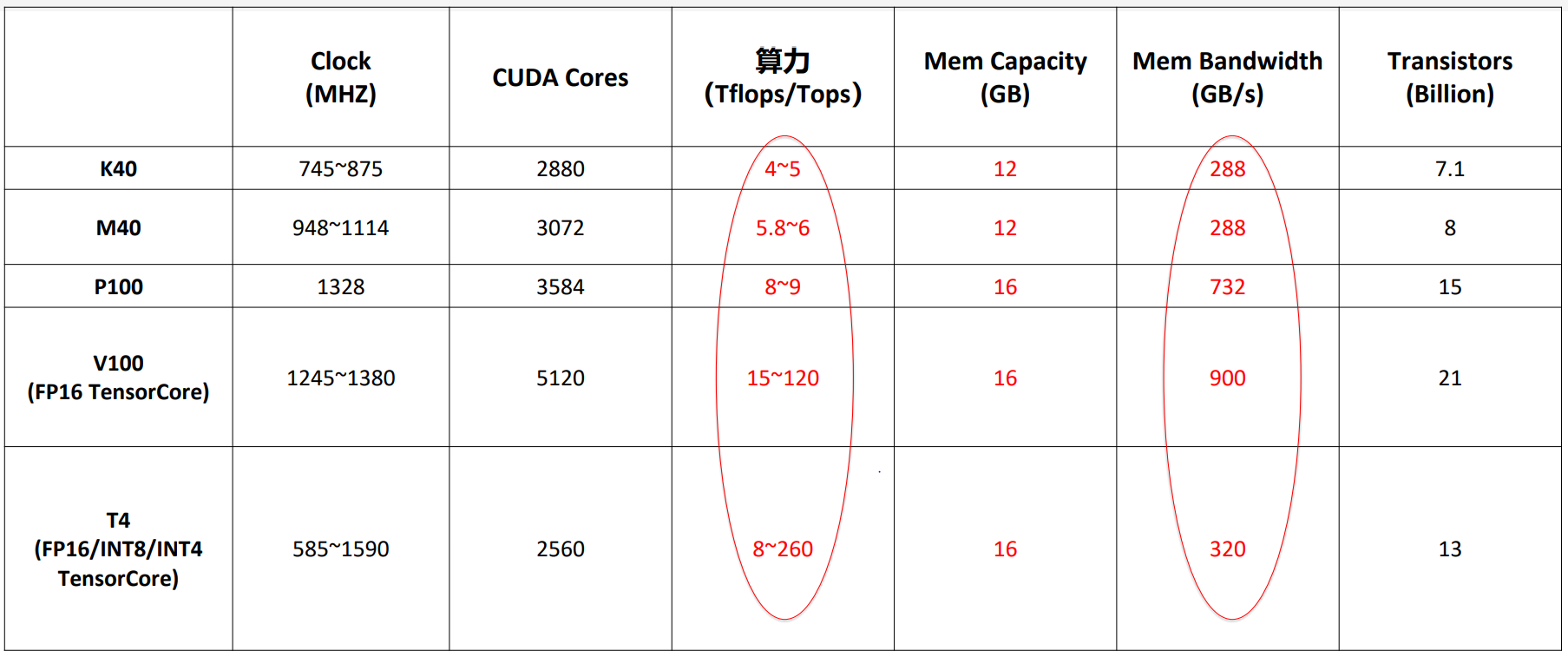
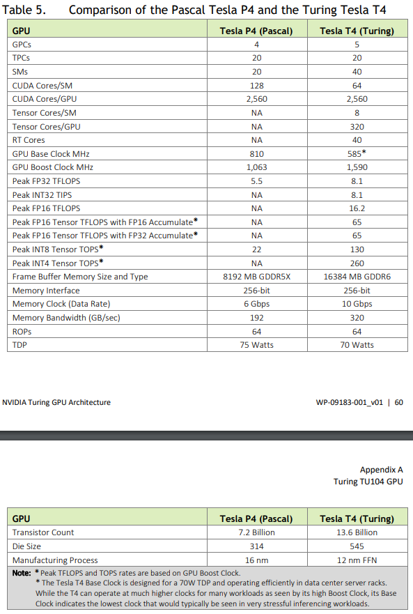
- SM中的每个Tensor Core可以在每个时钟周期内执行高达64次fp16输入融合浮点乘加运算(FMA),8个Tensor Core这可以在每个时钟周期内执行总计512次fp16乘加运算,或1024次fp运算。Turing新引入的INT8精度模式在每个时钟周期内更是可以执行2048个整数运算。Tesla T4身为Turing第一个使用Turing架构的GPU,包含2560个CUDA核心和320个Tensor Cores,可实现130 TOPs(Tera Operations per second)的int8运算和高达260 TOPs的int4运算。
附1:Turing架构机型T4相关数据
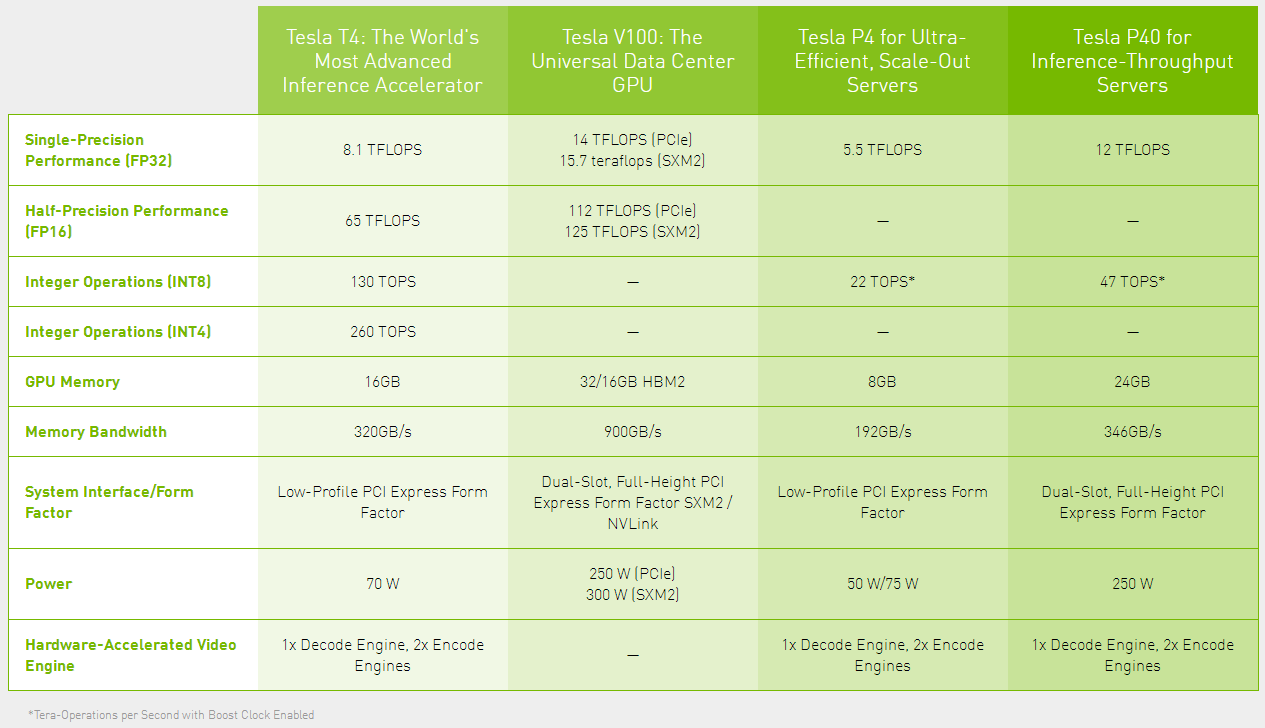
附2:Turing T4 vs Volta V100 vs Pascal P40比较