Note of Analog Circuit Book: Microelectronic Circuits by Sedra Smith
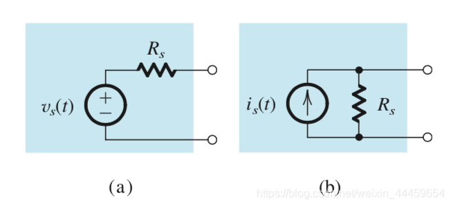
Norton and Thevenin Circuit
Find Equivalent Req:
Apply test source VT
Measure test current IT
Req = VT/IT.
Thevenin:
VTH=VOC
zero out independent sources (0 voltage = short circuit, 0 amplititude = open circuit)
Find RTH
Norton:
IN=VTH/RTH,RN=RTH
or short circuited, IN=IOC
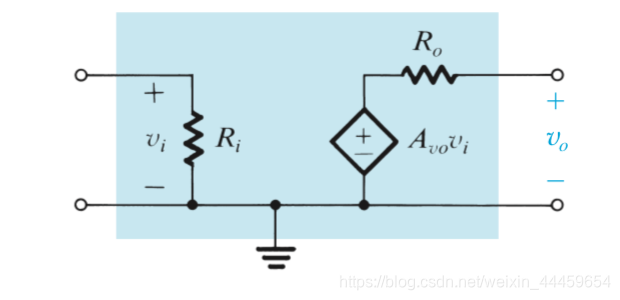
Amplifiers
Generic circuit model of Linear Amplifier
Rin= input resistance Rout= output resistance Avo= open loop voltage gain *Note: Linear amplifier will not change the frequency of input voltage.
vsvo=AvoRin+RsRinRL+RoutRL
desire: large Rin, small Rout, large Avo
Laplace Transform
A signal can be considered as considered as superpostion of many sinusoids. Time domain: v(t)=v0cos(ωt+ϕ) Frequency domain: Real part of v0∠ϕ
The formula for Laplace transform is: F(s)=∫t=0−+∞f(t)e−stdt,where s=jω, with requirement:
Integral must converge
f(t<0)=0
properties
Equation
Time dreivative
f′(t)⇔sF(s)−f(0+)
Convolution
F1(s)F2(s)⇔(f1∗f2)(t)=∫0tf1(τ)f2(t−τ)dt
Initial value theorem
f(0+)=lims→∞sF(s)
Final value theorem
f(∞)=lims→0sF(s)
In frequency domain, the impedance of L and C is L: Ls C:1/(Cs)
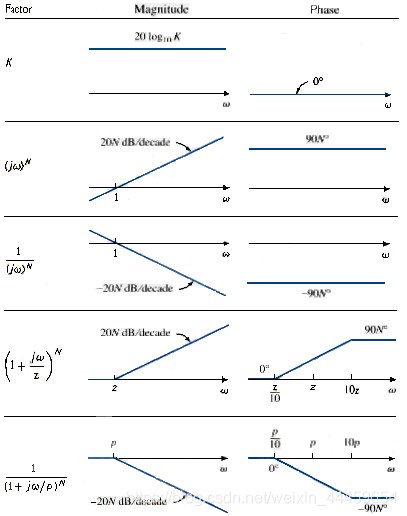
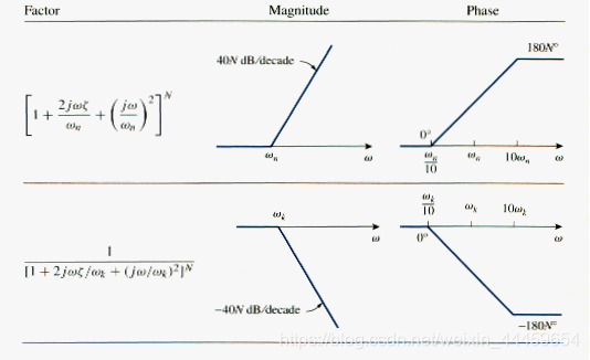
Bode Plot
How to draw bode plot:
Sallen & Key Method to Design Circuit
Essential Equation: T1=R1C1ω0 T2=R2C2ω0
Non-ideal Op-amps
Ideal Op-amp
Based on the Op-amp model, there are 3 assumptions:
A0→∞⇒v+=v−
Rin=∞⇒iin=0
Rout=0⇒ no voltage drop across Rout
3 basic configuration:
name
equ
Figure.
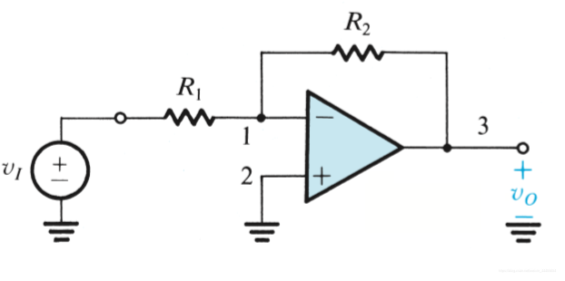
Inverting amplifier
vinvout=−R1R2
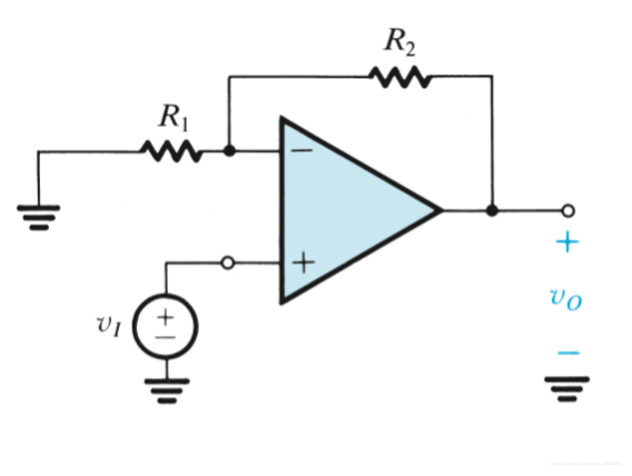
Non-inverting
vinvout=1+R1R2
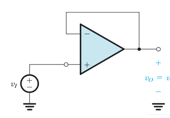
voltage folower
vinvout=1
Non-ideal Op-amp
Finite open-loop gain Non inverting: feed back factor f=R1+R2R1, vout/vin=1+A0fA0 Inverting: G=1+(1+R2/R1)/A0−R2/R1
Finite Rout̸=0 Turn off the input voltage source and find Rout′ Non-inverting amplifier: Rout′=1+A0fRout
Finite Rin i+=i−̸=0
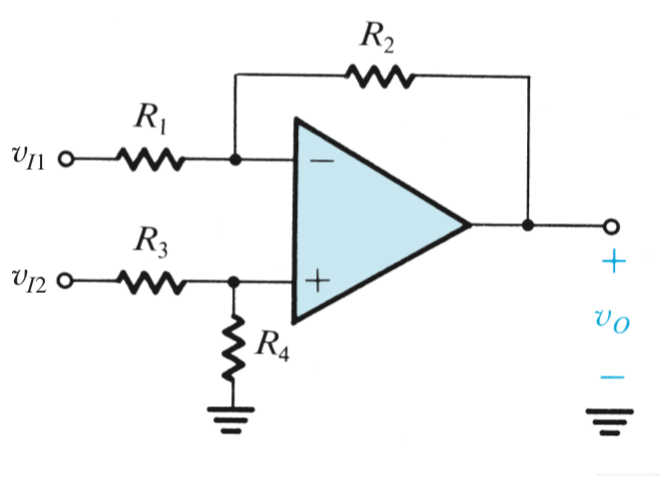
Common mode rejection ratio CMRR vid=v+−v− vic=2v++v− vout=A0[vid+CMRRvic], CMRR=AcmA0 Voltage follower: vinvout=1+A0(1−1/2CMRR)A0(1+1/2CMRR) Application: Difference Amplifier The circuit can be solved with superposition. To make it a differential amplifier, we ensure that R1R2=R3R4, through calculation, Ad=R1R2. If vI1=vI2=vIcm,
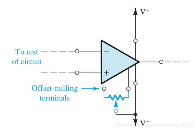
Input Offset Voltage Model the residual vout when vin=0 as a source at the input +: Modified vout=A0[vid+CMRRvic+vos] *this can be trimmed to zero by connecting a potentiometer to the two offset-nulling terminals.
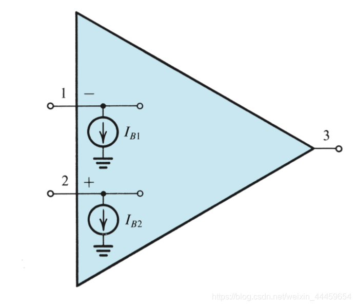
Input bias current IB1,IB2 are small constant current, IB1̸=IB2. Not the same as iin. IB=2IB1+IB2 IOS=∣IB1−IB2∣
Clipping Output is limited by +VCC and −VEE, introduce other frequency component.
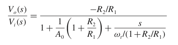
Bandwidth Open loop condition: open loop gain is frequency dependent A(s)=1+s/ωpA0 ωt= frequency when ∣A∣=1 ft=unity gain bandwidth Suppose ωt≫ωp, we have ωt=A0ωp Closed loop condition For inverting circuit: Assume A0≫1+R1R2, can get rid of the mid term. ω3dB=1+R2/R1ωt For non-inverting circuit: Note: gain-bandwidth product = ft.
Slew rate Come from the finite current available to charge and discharge internal capacitance. SR=dtdv0∣max Simple example: if vout(t)=vmsin(ωt), SR≥max(vout′(t))=vmω
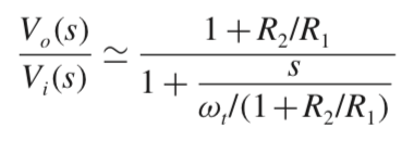
Internal of an Op-amp
v3=μGmR(v2−v1)
Diodes
p type (acceptor): positive charge carrier, releases as a “hole”. e.g. Boron(+3) n type (donor): negative charge carrier, mobile electron, e.g. Phosphorous(+5) concentration: number of charge carriers per unit volume([cm−3])
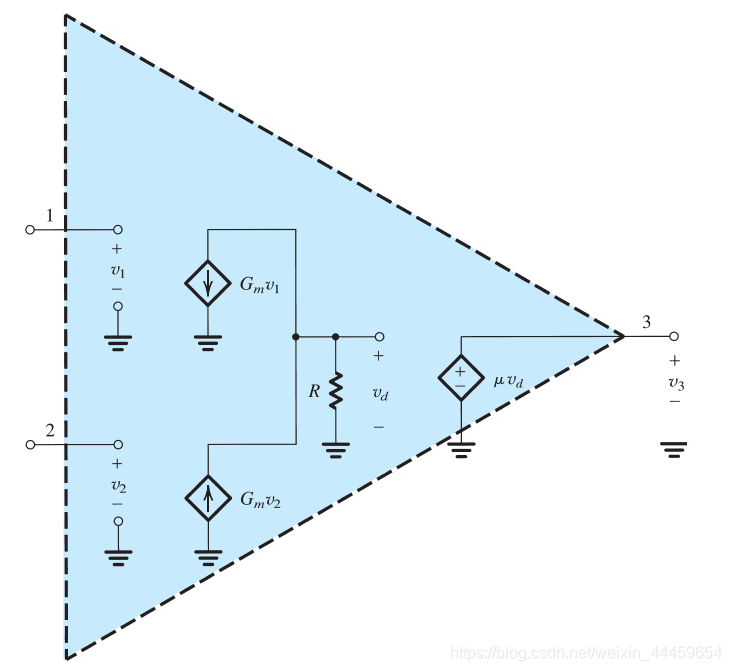
PN junction diode
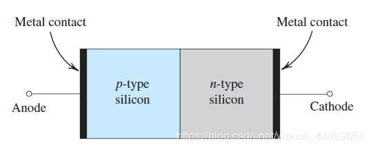
p type region has extra hole, and q type region has extra electron.
The hole will be filled with electrons gradually due to diffusion. The middle area is already charged, called depletion or space charge region.
An electromagnetic field formed. A built-in voltage was introduced, which stops diffusion. Emax=ϵsϵ0qNDxn=ϵsϵ0qNAxp, ϵs=electrical permittivity of silicon W=xn+xp=q2ϵsϵ0(1/NA+1/ND)(vbi−vA) vbi=qkBTln(ni2NDNA)
Apply positive voltage to p side, when vA>vbi, there will be no depletion area and large current can flow.
When a very large negative voltage applied, the junction will break down due to zener effect.
The I-V relation: ID=IS[eqvD/nkT−1]≈ISevD/vT=(under room temperature)IS[evD/0.0258−1]
Temperature Dependency
Forward Bias IS: doubles every 5∘C raise in temperature [Approximately Equivalent: VD decreases by 10mV, not very accurate]
Reverse Bias −IR: doubles for every 10∘C raise in temperature ID≈−IR(independent of voltage)