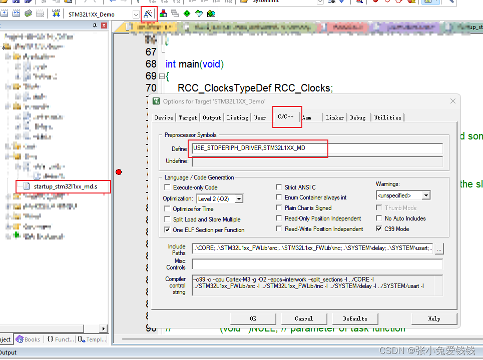
1. 我用的是STM32L151C8T6 的芯片,在github 上找了个别人的例程,拿来当模板改,由于他用的是HSE 外部晶振,我用的是内部晶振HSI,所以需要改系统时钟,改完后debug, 一直进不了main 函数,老以为是我改系统时钟改错了, 搞半天才找到原因,是printf 和微库 Use MicroLIB 的问题,keil 里面勾选就可以了
2. 改写系统初始化函数 void SetSysClock(void), 关闭HSE, 使用HSI
void SetSysClock(void)
{
    __IO uint32_t StartUpCounter = 0;
    __IO uint32_t HSEStatus = 0;

    __IO uint32_t HSIStartUpCounter = 0;
    __IO uint32_t HSIStatus = 0;

    /* SYSCLK, HCLK, PCLK2 and PCLK1 configuration ---------------------------*/
//    RCC->CR |= ((uint32_t)RCC_CR_HSEON); // Enable HSE
//    /* Wait till HSE is ready and if Time out is reached exit */
    do
//    {
//        HSEStatus = RCC->CR & RCC_CR_HSERDY;
//        StartUpCounter++;
//    } while ((HSEStatus == 0) && (StartUpCounter != HSE_STARTUP_TIMEOUT));
//    if ((RCC->CR & RCC_CR_HSERDY) != RESET)
//    {
//        HSEStatus = (uint32_t)0x01;
//    }
//    else
//    {
//        HSEStatus = (uint32_t)0x00;
//    }
//    if (HSEStatus == (uint32_t)0x01)
//    {
//        FLASH->ACR |= FLASH_ACR_ACC64; // Enable 64-bit access
//        FLASH->ACR |= FLASH_ACR_PRFTEN; // Enable Prefetch Buffer
//        FLASH->ACR |= FLASH_ACR_LATENCY; // Flash 1 wait state
//        RCC->APB1ENR |= RCC_APB1ENR_PWREN; // Power enable
//        PWR->CR = PWR_CR_VOS_0; // Select the Voltage Range 1 (1.8 V)
//        while((PWR->CSR & PWR_CSR_VOSF) != RESET) // Wait Until the Voltage Regulator is ready
//        {
//        }
//        RCC->CFGR |= (uint32_t)RCC_CFGR_HPRE_DIV1; // HCLK = SYSCLK /1
//        RCC->CFGR |= (uint32_t)RCC_CFGR_PPRE2_DIV1; // PCLK2 = HCLK /1
//        RCC->CFGR |= (uint32_t)RCC_CFGR_PPRE1_DIV1; // PCLK1 = HCLK /1
//        /*  PLL configuration */
//        RCC->CFGR &= (uint32_t)((uint32_t)~(RCC_CFGR_PLLSRC | RCC_CFGR_PLLMUL | RCC_CFGR_PLLDIV));
//        RCC->CFGR |= (uint32_t)(RCC_CFGR_PLLSRC_HSE | RCC_CFGR_PLLMUL12 | RCC_CFGR_PLLDIV3);
//        RCC->CR |= RCC_CR_PLLON; // Enable PLL
//        while((RCC->CR & RCC_CR_PLLRDY) == 0) // Wait till PLL is ready
//        {
//        }
//        /* Select PLL as system clock source */
//        RCC->CFGR &= (uint32_t)((uint32_t)~(RCC_CFGR_SW));
//        RCC->CFGR |= (uint32_t)RCC_CFGR_SW_PLL;
//        while ((RCC->CFGR & (uint32_t)RCC_CFGR_SWS) != (uint32_t)RCC_CFGR_SWS_PLL) // Wait till PLL is used as system clock source
//        {
//        }
//    }
//    else // HSE startup fail, then use HSI as system clock source
//    {
        RCC->CR |= RCC_CR_HSION; // enable HSI as system clock source
        do
        {
            HSIStatus = RCC->CR & RCC_CR_HSIRDY;
            HSIStartUpCounter++;
        } while ((HSIStatus == 0) && (HSIStartUpCounter != HSI_STARTUP_TIMEOUT)); // Wait till HSI is ready and if Time out is reached exit
        if ((RCC->CR & RCC_CR_HSIRDY) != RESET)
        {
            HSIStatus = (uint32_t)0x01;
        }
        else
        {
            HSIStatus = (uint32_t)0x00;
        }
        if (HSIStatus == (uint32_t)0x01)
        {
            FLASH->ACR |= FLASH_ACR_ACC64; // Enable 64-bit access
            FLASH->ACR |= FLASH_ACR_PRFTEN; // Enable Prefetch Buffer
            FLASH->ACR |= FLASH_ACR_LATENCY; // Flash 1 wait state
            RCC->APB1ENR |= RCC_APB1ENR_PWREN; // Power enable
            PWR->CR = PWR_CR_VOS_0; // Select the Voltage Range 1 (1.8 V)
            while((PWR->CSR & PWR_CSR_VOSF) != RESET) // Wait Until the Voltage Regulator is ready
            {
            }
            RCC->CFGR |= (uint32_t)RCC_CFGR_HPRE_DIV1; // HCLK = SYSCLK /1
            RCC->CFGR |= (uint32_t)RCC_CFGR_PPRE2_DIV1; // PCLK2 = HCLK /1
            RCC->CFGR |= (uint32_t)RCC_CFGR_PPRE1_DIV1; // PCLK1 = HCLK /1

            /*  PLL configuration */
            RCC->CFGR &= (uint32_t)((uint32_t)~(RCC_CFGR_PLLSRC | RCC_CFGR_PLLMUL | RCC_CFGR_PLLDIV));
            RCC->CFGR |= (uint32_t)(RCC_CFGR_PLLSRC_HSI | RCC_CFGR_PLLMUL4 | RCC_CFGR_PLLDIV2);

            RCC->CR |= RCC_CR_PLLON; // Enable PLL
            while((RCC->CR & RCC_CR_PLLRDY) == 0) // Wait till PLL is ready
            {
            }

            /* Select PLL as system clock source */
            RCC->CFGR &= (uint32_t)((uint32_t)~(RCC_CFGR_SW));
            RCC->CFGR |= (uint32_t)RCC_CFGR_SW_PLL;
            while ((RCC->CFGR & (uint32_t)RCC_CFGR_SWS) != (uint32_t)RCC_CFGR_SWS_PLL) // Wait till PLL is used as system clock source
            {
            }
        }
        else
        {
            // HSI startup fail
        }
//    }
}
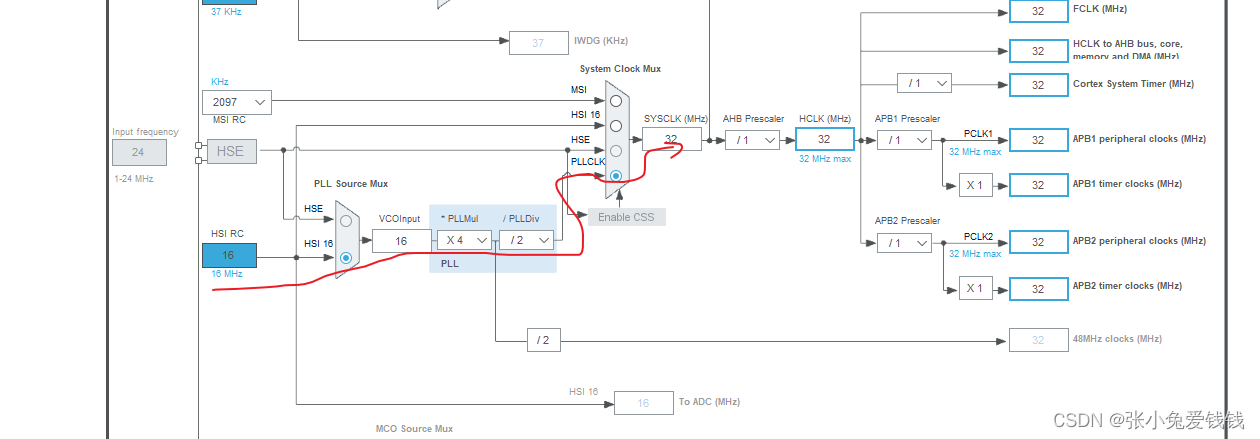
3. STM32L151C8T6 系统时钟树,在STM32CubeMX 软件里面可以看的到
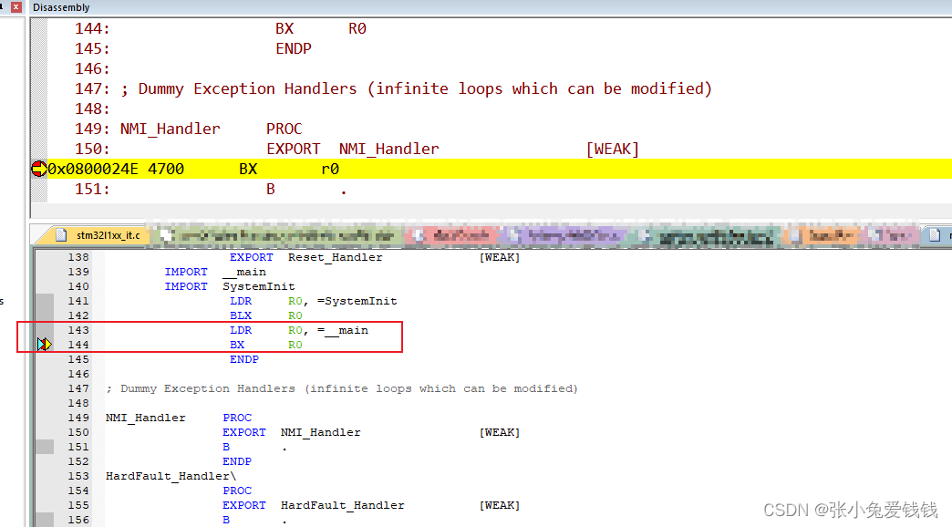
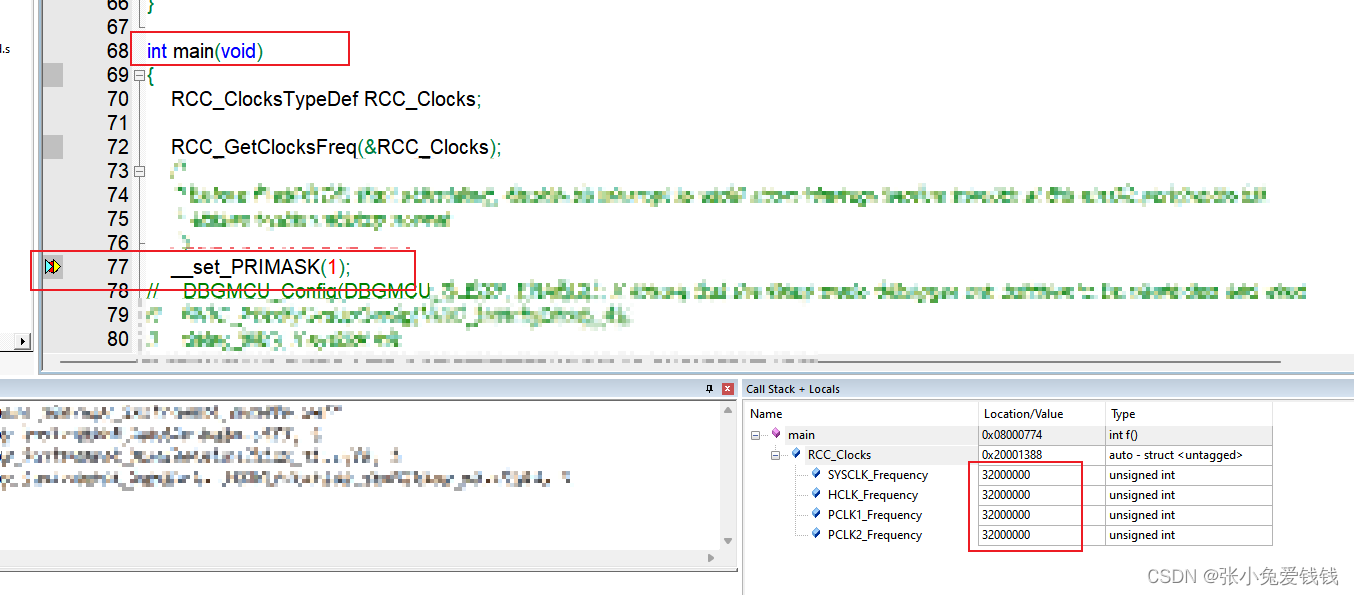
4. Debug 的时候一直卡在这个地方
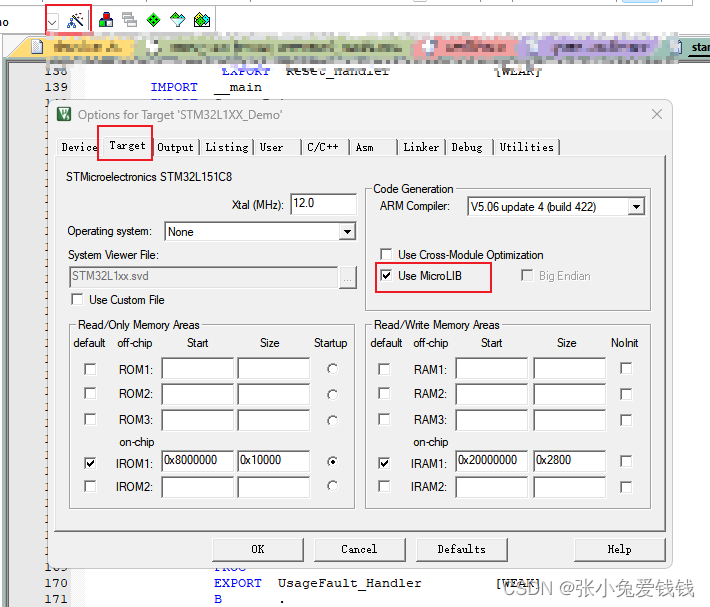
5. 勾选微库,重新编译,再debug调试就OK了
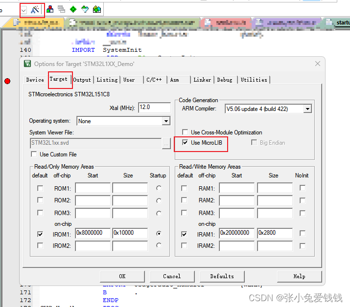
6. 或者不勾选微库也行,禁用半主机模式就可以了
7. 跟fputc 没关系的, 重新编译,调试就可以了,查看系统各个总线的时钟
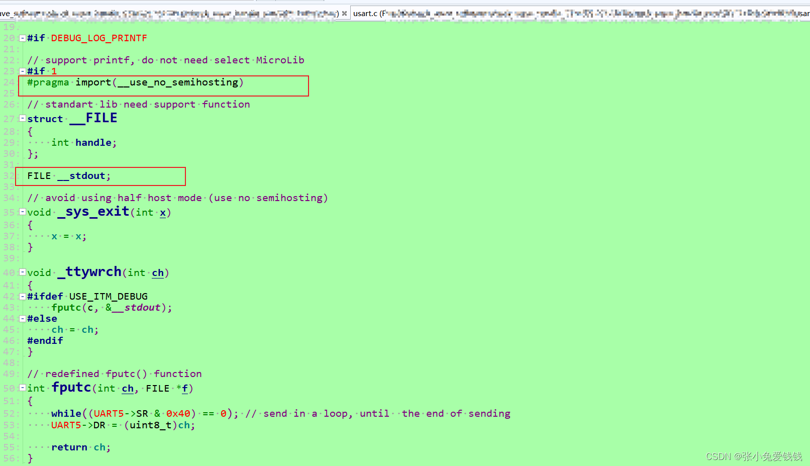
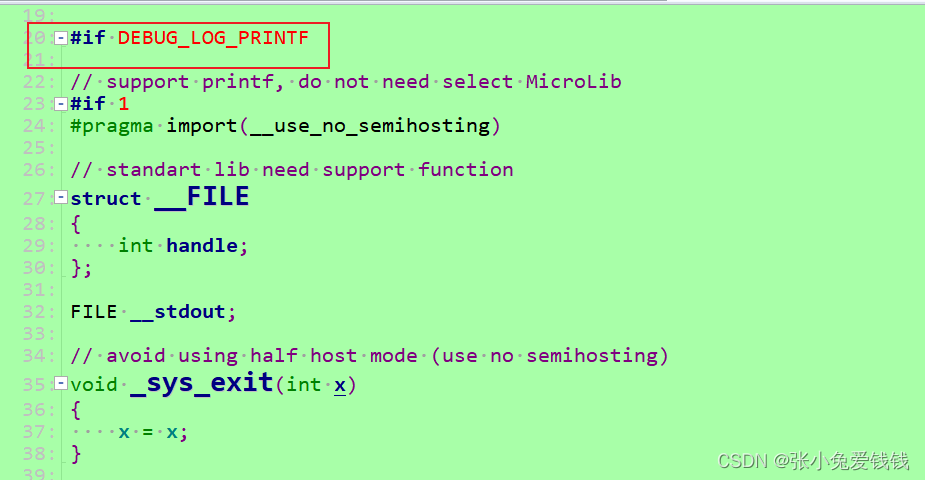
8. 我的问题是这个宏没有打开,导致下面的代码都没有编译进来,也就没有禁用半主机模式,没注意看他还在这里加了一个日志宏开关,我直接把他干掉了,坑爹的玩意
9. 启动文件,系统宏配置