原文:http://www.eefocus.com/antaur/blog/17-08/423754_f75f7.html
0.引言
在上一节中,为了验证AXI4-Lite总线读写时序,创建了一个主从机直连的系统,并进行了行为仿真。该系统并没有经过总线控制器,因此不能算一个完整的主从机总线通信验证系统。
本节计划创建一个通过总线控制器交互的主从模块通信系统,其中主从模块皆有PL编码实现,同时工程要下板验证,因此需要设计外设,用于信息交互。
1.工程规划

其中,从机IP核与实验3中定义的类似,包含拨码开关的状态采样和LED的驱动显示。只是主机由CPU转换成PL编写的Master了。
主机端在检测到按键跳变沿触发后,启动读取流程,由从机的reg[3:0] A中获取拨4个码开关的状态。读取得到的数据经过简单的字符变换,启动写入流程,将其写入到从机端的寄存器reg[3:0] B中,驱动LED灯显示。
2.主从机Verilog编码
主从机的接口框架均由向导产生,再其基础上进行代码改造。其中从机端的Verilog编码见附录1,主机端的Verilog编码见附录2。其中主机端的示例程序代码将AXI4-Lite总线读写业务与用户逻辑业务深度耦合,因此主机端的代码修改幅度比较大。修改完之后,需要进行行为仿真,从而确保修改的代码逻辑是正确的。
此时测试方案同上一节一样,利用主从机直连的方式构建一个测试系统,进行行为仿真,直连系统代码见附录3,仿真文件代码见附录4。
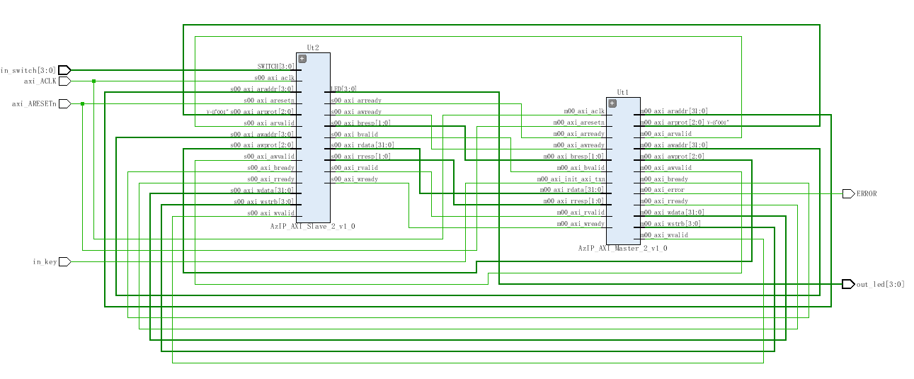
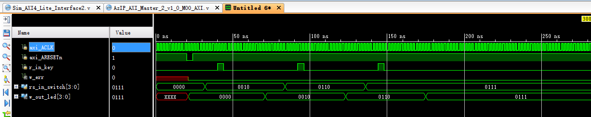
其中附录3构建的系统RTL级图和仿真结果如下图所示。可以虽然IP核代码经过了大改,但是由于已经明确的读写时序逻辑,编码的难度并不大,从结果可以看出逻辑功能是正确的。
之后就可以进行下一步,构建Block Design设计了。
3.构建SoC系统
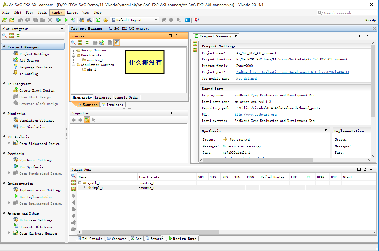
Step1: 创建工程
重新创建一个Vivado工程,打开之后,可以看到什么都没有。
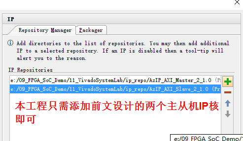
Step2: 绑定用户IP核路径
按照前面的学习,应该创建“Block Design”,但是在此之间,一定要先完成下面步骤,即需要将用户设计的IP核添加到工程库中,具体操作如下:
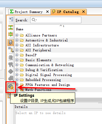
点击图中按钮,配置IP参数。
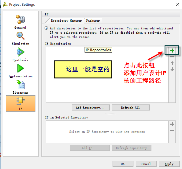
点击OK按钮保存配置然后退出。
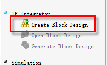
Step3: 设计Block Design
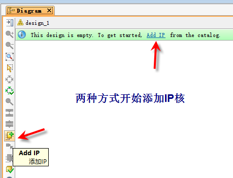
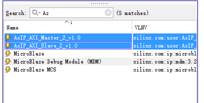
选择需要的两个IP核,回车确认。
此时,在Block Design页面中会放置选中的IP核模块。

点击“Run Connection Automation”系统会自动添加AXI4总线控制器。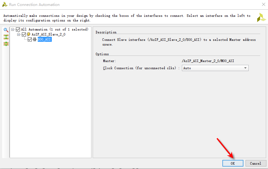
保持默认点击OK即可,自动构建出响应的包含总线控制器的系统。
排布整形以后得到如下设计方案。
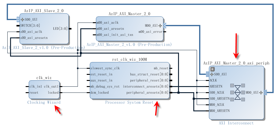
排布整形以后得到如下设计方案。

该方案就是我们预期的设计结果。
之后创建外部端口。结果如下:
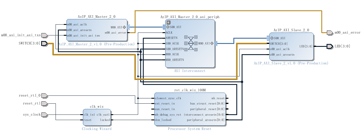

可以看出方案是没有问题的。
查看地址设置

在系统中,对于总线控制器默认的基地址配置为0x44A0_0000,而主机IP核代码中默认的目标地址为

因此,这里也修改为0x4000_0000.
Step4: 将Block Design转换为Verilog封装
在Source页面中,选中Block Design文件,在右键菜单中选择“Create HDL Wrapper...”,
选择下图所示配置
系统会在Block Design之上创建一个Verilog的封装。并自动将其设为顶层文件。
Step5: 设计约束文件(主要是管脚约束)
首先对工程进行综合。

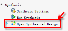
综合无误后双击下图所示按钮,代开“Synthesized Design”
选择“I/O Planning”页面

具体配置如下:
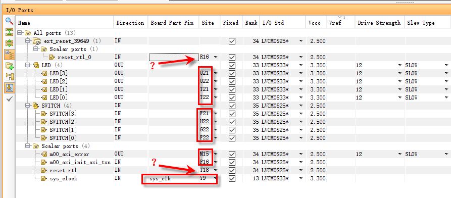
问题是两个复位信号的极性现在不确定,上图绑定的是开发板上的按键开关,是正脉冲,有待确定。
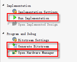
Step6: Implementation & IP核修改
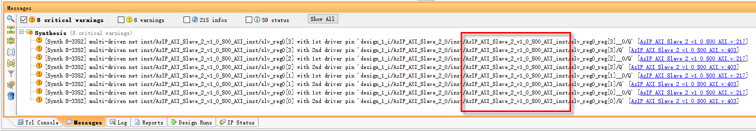
但是Implementation执行完毕之后,报错,显示信息如下:
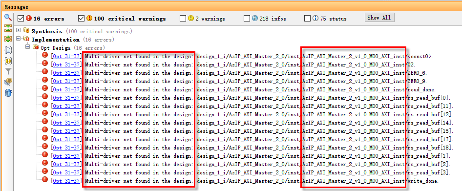
可以看出错误原因都是多驱动源,出错的模块都是主机端的底层模块。但是Synthesis时系统没有报错啊?Reset Implementation Run然后Reset Synthesis Run(操作入口如下)后,清除整个编译过程,然后重新Run Synthesis。

查看Message页面,没有Error信息,但有100个Critical warnings信息,查看内容如下:
可以看出,综合完的Critical warning必须处理,否者将会触发后继操作发生error。
查看代码,发现针对本例程,该错误的原因是一个reg在多个always中进行了非阻塞性赋值,虽然是在一个module中,并且各个always块的触发条件均相同,但是系统在进行后台分析时,仍会认为发生错误,以read_done寄存器为例。发生异常的代码如下:
【个人分析心得】
在同一个module中,同一个reg可以在不同的always中进行读取判断,但是不能在不同的always中对其赋值。
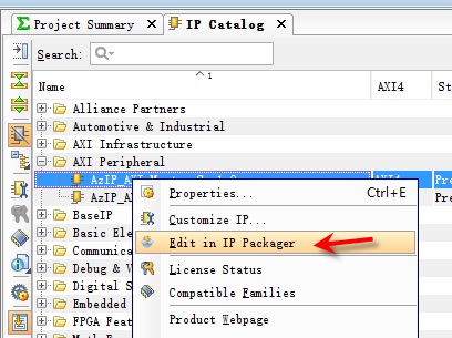
修改IP核的源代码只能利用IP catalog中的Edit in IP Packager,操作入口如下(详见学习笔记2)。
修改完的代码如附录5所示,综合完之后Message页面显示结果如下:
已经没有Critial Warnings信息了。
之后重新封装该IP核。
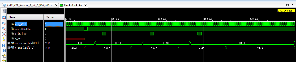
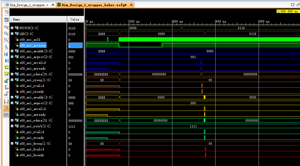
然后重新仿真主机和从机直连的测试工程,运行仿真测试,下面给出了整体模块的对外端口仿真结果和总线时序仿真结果。
从整体模块的对外端口仿真结果可以看出,拨码开发的采样结果(rs_in_switch[3:0])在主机触发按键in_key的出发后,被系统发送给LED显示(w_out_led[3:0]),结果是正确的。
从总线时序仿真结果可以看出,每次按钮in_key触发后,都经过了一次读操作核1次写操作而且总线时序是正确的。而且通过上面的整体模块的对外端口仿真结果表明:基本上每怎么改动的从机模块能够正常响应经过大改的主机模块发送的读写操作。
顶层模块仿真结果如下
总线时序仿真结果如下:

由于IP核本身经过重新封装,此时再次打开挂载总线控制器的SoC工程的Block Design,可以在页面上方显示如下提示信息,表示Vivado软件检测到使用的IP核发生了变动,提示用户进行更新。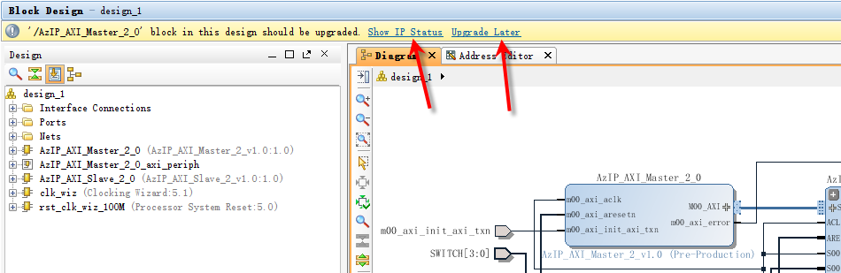
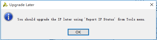
点击“Upgrade Later”提示需要在下面的Report IP Status页面进行更新。
点击“Show IP Status”将弹出下列页面,可以显示IP核的更新信息。点击下方的“Update Selected”按钮,将会将会自动更新IP核的信息。
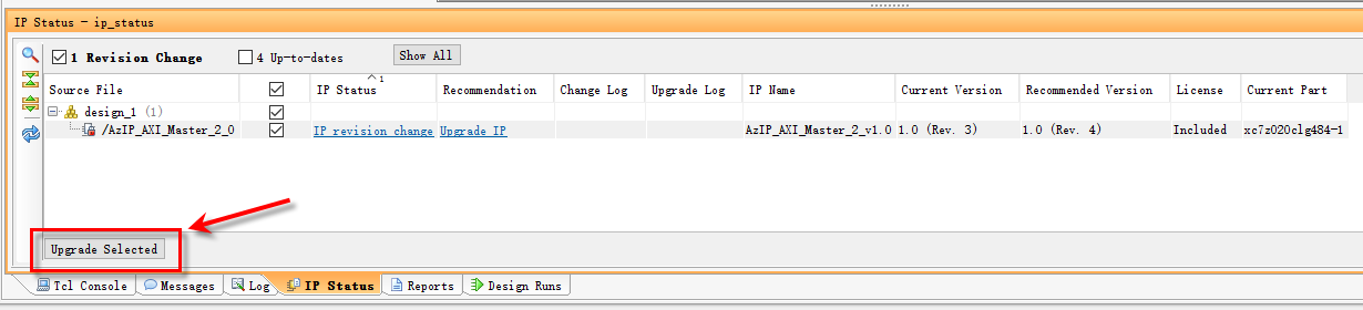
更新完毕显示如下信息:
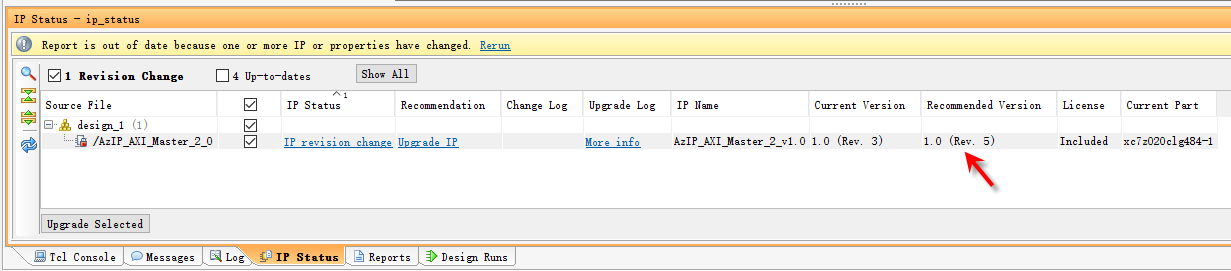
点击Return,显示如下信息:
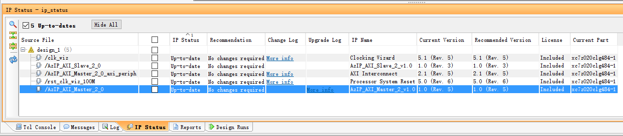
由于本次对于IP核的修改,仅限于底层代码,对于IP核的外围管脚封装并没有做任何修改,因此Block Design本身并没有什么变化,仅仅是引用的IP核发生了更新。
删除原有的HDL Wrapper,生成新的HDL Wrapper顶层模块。
综合完成之后,报警出现8个critical warning,具体信息如下:
原因同样是多个驱动源,但是出现问题的已经变成从机模块了,主机模块已经没有critical warning了。而从机模块基本上没有什么改动,以向导生成的为准,因此暂时不考虑,执行Run implementation
但是运气不好,Run implementation没有执行过去,报了4个error。
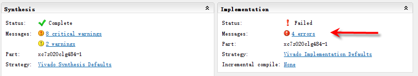
具体查看信息如下:
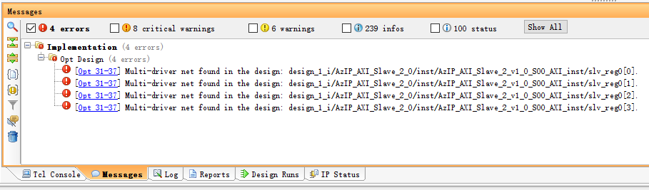
还需要重新修改从机的IP核。修改流程跟上述一致,修改后的从机源代码见附录6,修改完从机后,一定要经过直连系统的功能仿真确保修改代码时没有影响整体业务逻辑。
之后对SoC系统中的block Design进行Upgrate Select IP,之后更新HDL wrapper,之后Run Synthesis,Run Implementation。结果如下,终于通过了Implementation。

Step7:SoC系统的行为仿真
本人在实际练习时,首先没有经过这一步操作,而是直接下板,发现并没有任何反应,因此才反过来重新做SoC系统的行为仿真。
仿真测试文件的源代码见附录7。
(1)Clock Wizard模块时序仿真
该模块是系统自带的始终模块,等同于V4时使用的dcm模块,能够实现时钟分频操作。
通过仿真确定,其复位信号reset为正脉冲复位,低电平工作,locked高电平表示锁定。
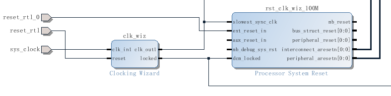

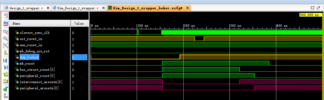
(2)Processor System Reset模块时序仿真
该模块的官方文档为PG-164,功能简介如下:


能够为SoC系统的各种模块产生满足时序要求的复位信号。

官方文档上的时序示意图如下所示:
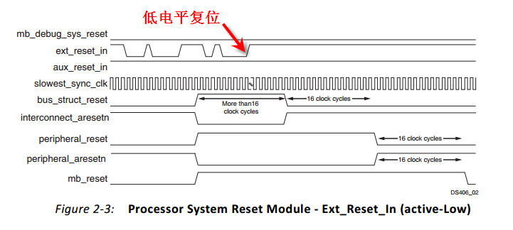
可以看出:ext_reset_in为负脉冲复位,而前文构建系统进行管脚约束时,约束的是ZedBoard板上的按键,而按键本身时正脉冲,逻辑正好反了。这个需要修改。
仿真时,构建复位信号为负脉冲。得到该模块的仿真结果如下:
(3)主机IP模块的总线时序仿真
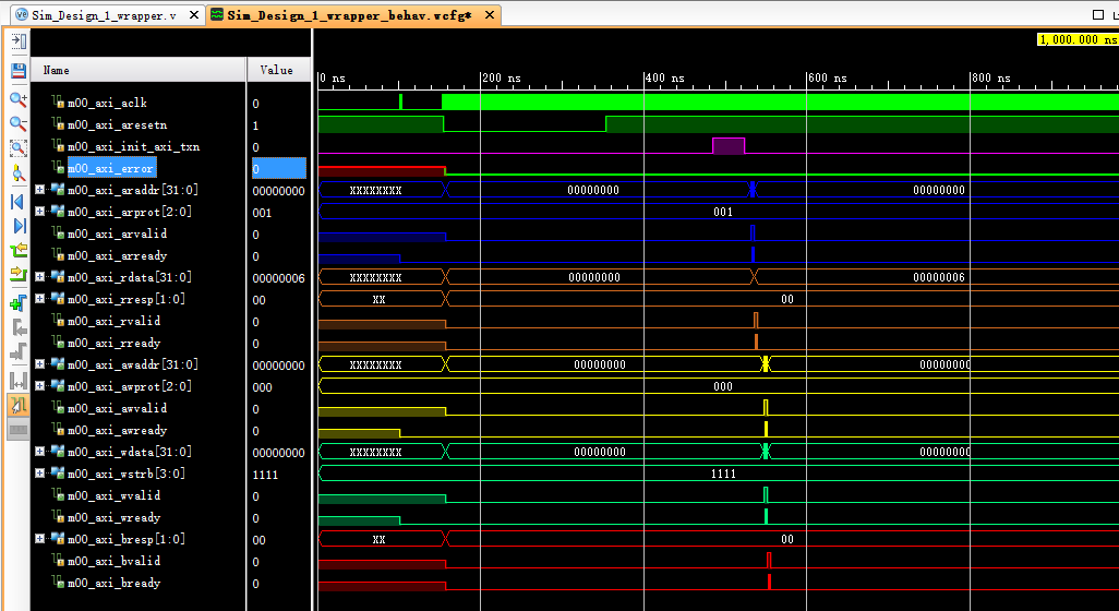
可以看出,主机IP核模块在axi_txn信号正脉冲的触发下,先发起了读操作,而后进行了写操作。
将上图读写操作区间放大,观察数据内容,得到的仿真图如下所示:
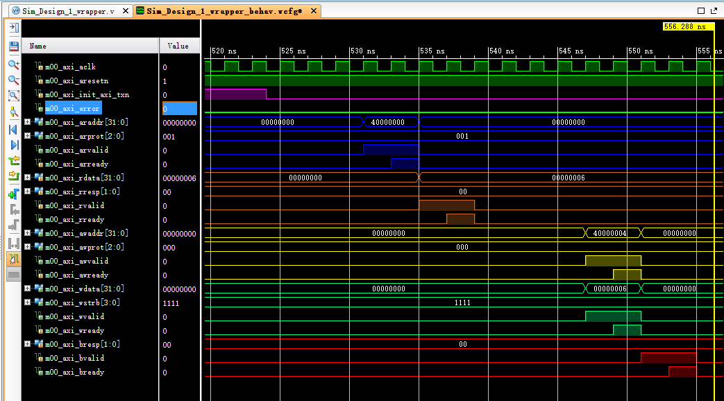
可以看到,主机向从机地址为0x4000_0000的寄存器中读取数据,读到的数据为0x0000_00006。
而后主机向从机地址为0x4000_0004的寄存器写入数据,数据为0x0000_0006.
主机上的总线时序是正确的。
(4)从机IP模块的总线时序仿真
从上图可以看出,从机先被主机读取,而后接收主机写入操作,可以看到拨码开关输入的是0x0110,通过总线读取操作,输出的还是0x0110。表示整个系统逻辑功能时正确的。
放大读写操作时的仿真图如下所示:
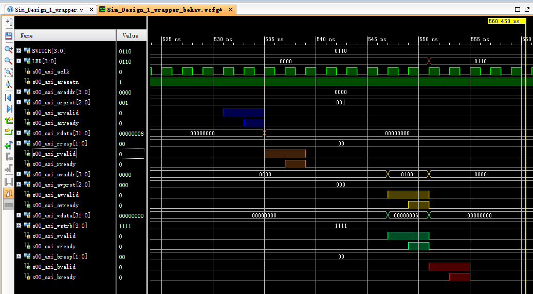
主机发起的读取操作的读地址为0x4000_0000,经过总线控制器,去除了高位的段地址,只留下低4位的Offset Address(0000二进制)发送给从机模块用以模块内区分寄存器。但是从机响应读操作,返回的数据仍为32bits,数值为0x0000_0006,即为拨码开关输入的数据。
写操作时,主机发出的地址为0x4000_0004,经过总线控制器,去除了高位的段地址,只留下低4位的Offset Address(0100二进制,对应0x4十六进制)发送给从机模块用以模块内区分寄存器。同时写入的数据为32bits,数值为0x0000_0006。用以驱动LED灯显示。
(5)多次读写操作仿真
为了验证系统对于重复操作响应的正确性,修改仿真文件,实现多次读写,仿真结果如下:

上图证明,SoC系统对于重复性触发操作是正确的。
Step8: 根据系统仿真结果对前文实现系统进行修正
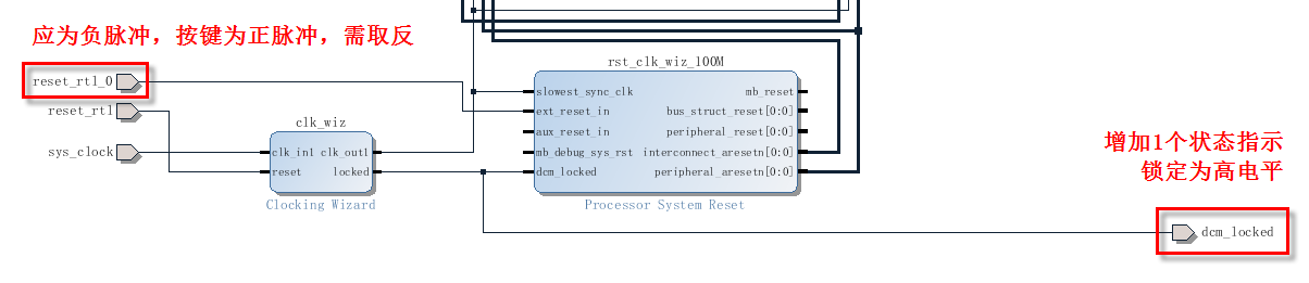
其中,对于reset_rtl_0取反,原想在HDL Wrapper的verilog代码中进行,但是综合后系统会自动重新生成HDL Wrapper,手动修改的取反又被更正回来了。
处理方法有两种:
一种是再封装一个顶层模块,在其中添加取反操作(没有尝试),这种方法需要根据新的顶层文件重新配置管脚约束。
另一种是再block design中添加一个反相器,可以用已有IP核(该IP名称为Utility Vector Logic),该IP核可以配置,配置界面如下:
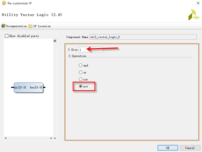
完成后的block design方案如下:
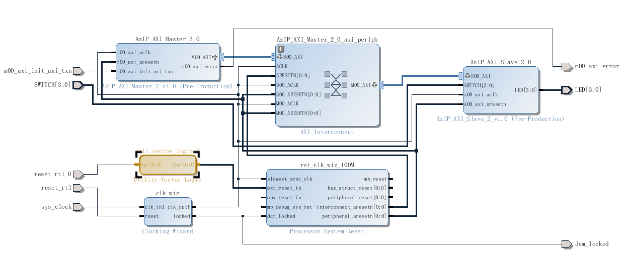
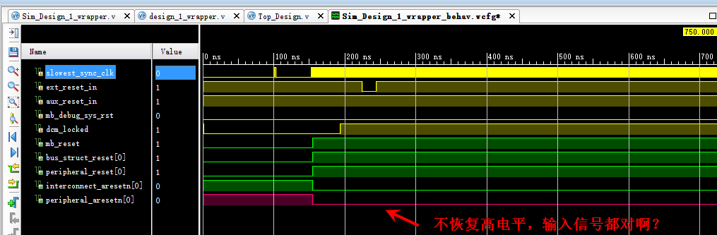
【结果说明】:这种方案,直接下板任然没有反应,通过系统仿真,结果如下,对于“Processor System Reset”模块,输入信号与正常时都是一样的,但就是输出复位信号不恢复。真是怪了去了。原因暂时没找到。
最后采用第一种方法,添加顶层文件,并在其中对reset_rtl_0信号取反。
【结果说明】:这种方案下板成功!!!!!
添加一个DCM_LOCKED管脚,将其绑定到一个LED上,当该LED灯亮时,表示DCM工作正常。
对应的新的管脚约束配置如下:

Step8: Generate BitStream & 下板测试
本示例中,向Zynq芯片下载的工程全部位于PL端,与基本纯HDL工程下载操作是一致的。
BitStream文件生成成功之后,启动“Hardware Manager”,在打开的页面中显示如下信息:
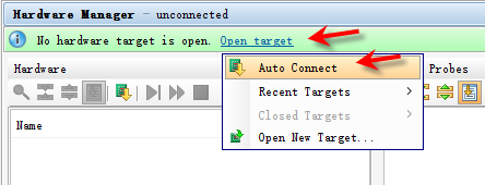
连接好开发板,并正常供电,然后点击“Open target”后,弹出图中所示菜单,选择“Auto Connect”系统自动扫描JTAG链。
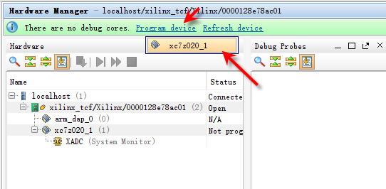
点击“Program device”并选择响应的芯片,弹出配置界面信息。
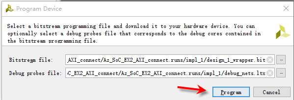
确认无误后,点击“Program”按钮,开始下载程序。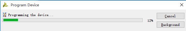
【结论】下板运行成功,符合设计要求。
附录1:主机IP模块底层源码--存在Multi-driver问题
`timescale 1 ns / 1 ps
module AzIP_AXI_Master_2_v1_0_M00_AXI #
(
// Users to add parameters here
// User parameters ends
// Do not modify the parameters beyond this line
// The master requires a target slave base address.
// The master will initiate read and write transactions on the slave with base address specified here as a parameter.
parameter C_M_TARGET_SLAVE_BASE_ADDR = 32'h40000000,
// Width of M_AXI address bus.
// The master generates the read and write addresses of width specified as C_M_AXI_ADDR_WIDTH.
parameter integer C_M_AXI_ADDR_WIDTH = 32,
// Width of M_AXI data bus.
// The master issues write data and accept read data where the width of the data bus is C_M_AXI_DATA_WIDTH
parameter integer C_M_AXI_DATA_WIDTH = 32,
//
parameter C_OFFSET_READ_REG_ADDR = 32'h0000_0000,
parameter C_OFFSET_WRITE_REG_ADDR = 32'h0000_0004
)
(
// Do not modify the ports beyond this line
// Initiate AXI transactions
input wire INIT_AXI_TXN,
// Asserts when ERROR is detected
output wire ERROR,
///////////////////////////////////////////////////////////////////////////////////////
// AXI clock signal
input wire M_AXI_ACLK,
// AXI active low reset signal
input wire M_AXI_ARESETN,
///////////////////////////////////////////////////////////////////////////////////////
// Master Interface Write Address Channel ports. Write address (issued by master)
output wire [C_M_AXI_ADDR_WIDTH-1 : 0] M_AXI_AWADDR,
// Write channel Protection type.
// This signal indicates the privilege and security level of the transaction,
// and whether the transaction is a data access or an instruction access.
output wire [2 : 0] M_AXI_AWPROT,
// Write address valid.
// This signal indicates that the master signaling valid write address and control information.
output wire M_AXI_AWVALID,
// Write address ready.
// This signal indicates that the slave is ready to accept an address and associated control signals.
input wire M_AXI_AWREADY,
///////////////////////////////////////////////////////////////////////////////////////
// Master Interface Write Data Channel ports. Write data (issued by master)
output wire [C_M_AXI_DATA_WIDTH-1 : 0] M_AXI_WDATA,
// Write strobes.
// This signal indicates which byte lanes hold valid data.
// There is one write strobe bit for each eight bits of the write data bus.
output wire [C_M_AXI_DATA_WIDTH/8-1 : 0] M_AXI_WSTRB,
// Write valid. This signal indicates that valid write data and strobes are available.
output wire M_AXI_WVALID,
// Write ready. This signal indicates that the slave can accept the write data.
input wire M_AXI_WREADY,
///////////////////////////////////////////////////////////////////////////////////////
// Master Interface Write Response Channel ports.
// This signal indicates the status of the write transaction.
input wire [1 : 0] M_AXI_BRESP,
// Write response valid.
// This signal indicates that the channel is signaling a valid write response
input wire M_AXI_BVALID,
// Response ready. This signal indicates that the master can accept a write response.
output wire M_AXI_BREADY,
///////////////////////////////////////////////////////////////////////////////////////
// Master Interface Read Address Channel ports. Read address (issued by master)
output wire [C_M_AXI_ADDR_WIDTH-1 : 0] M_AXI_ARADDR,
// Protection type.
// This signal indicates the privilege and security level of the transaction,
// and whether the transaction is a data access or an instruction access.
output wire [2 : 0] M_AXI_ARPROT,
// Read address valid.
// This signal indicates that the channel is signaling valid read address and control information.
output wire M_AXI_ARVALID,
// Read address ready.
// This signal indicates that the slave is ready to accept an address and associated control signals.
input wire M_AXI_ARREADY,
///////////////////////////////////////////////////////////////////////////////////////
// Master Interface Read Data Channel ports. Read data (issued by slave)
input wire [C_M_AXI_DATA_WIDTH-1 : 0] M_AXI_RDATA,
// Read response. This signal indicates the status of the read transfer.
input wire [1 : 0] M_AXI_RRESP,
// Read valid. This signal indicates that the channel is signaling the required read data.
input wire M_AXI_RVALID,
// Read ready. This signal indicates that the master can accept the read data and response information.
output wire M_AXI_RREADY
);
// Example State machine to initialize counter, initialize write transactions,
// initialize read transactions and comparison of read data with the
// written data words.
parameter [1:0] IDLE = 2'b00, // 空闲状态,等待按键触发
INIT_READ = 2'b01, // 读取从机数据
INIT_TRANS = 2'b11, // 读写数据间的字符变换
INIT_WRITE = 2'b10; // 向从机发送处理后的数据
reg [1:0] mst_exec_state; // 状态机寄存器
///////////////////////////////////////////////////////////////////////////////////////
// AXI4LITE 总线可控输出信号
// [1] Write Address Channel
reg [C_M_AXI_ADDR_WIDTH-1 : 0] axi_awaddr; //write address
reg axi_awvalid; //write address valid
assign M_AXI_AWADDR = axi_awaddr;
assign M_AXI_AWPROT = 3'b000;
assign M_AXI_AWVALID = axi_awvalid;
// [2] Write Data Channel
reg [C_M_AXI_DATA_WIDTH-1 : 0] axi_wdata; //write data
reg axi_wvalid; //write data valid
assign M_AXI_WDATA = axi_wdata;
assign M_AXI_WSTRB = 4'b1111;
assign M_AXI_WVALID = axi_wvalid;
// [3] Write Response Channel
reg axi_bready; //write response acceptance
assign M_AXI_BREADY = axi_bready;
// [4] Read Address Channel
reg [C_M_AXI_ADDR_WIDTH-1 : 0] axi_araddr; //read addresss
reg axi_arvalid; //read address valid
assign M_AXI_ARADDR = axi_araddr;
assign M_AXI_ARPROT = 3'b001;
assign M_AXI_ARVALID = axi_arvalid;
// [5] Read Data Channel
reg axi_rready; //read data acceptance
assign M_AXI_RREADY = axi_rready;
///////////////////////////////////////////////////////////////////////////////////////
// AXI4LITE 总线异常状态指示
wire write_resp_error;//Asserts when there is a write response error
wire read_resp_error;//Asserts when there is a read response error
//The error register is asserted when any of the write response error, read response error or the data mismatch flags are asserted.
reg error_reg;
assign ERROR = error_reg;
///////////////////////////////////////////////////////////////////////////////////////
// 用户逻辑寄存器
// 触发按键跳变沿检测
reg init_txn_ff;
reg init_txn_ff2;
wire init_txn_pulse;
// 按键是正脉冲,检测按键的下升沿
assign init_txn_pulse = (!init_txn_ff) && init_txn_ff2;
always @(posedge M_AXI_ACLK)
begin
// Initiates AXI transaction delay
if (M_AXI_ARESETN == 0 ) begin
init_txn_ff <= 1'b0;
init_txn_ff2 <= 1'b0;
end
else begin
init_txn_ff <= INIT_AXI_TXN;
init_txn_ff2 <= init_txn_ff;
end
end
///////////////////////////////////////////////////////////////////////////////////////
// 用户逻辑寄存器
reg [C_M_AXI_DATA_WIDTH-1 : 0] rs_read_buf; // 定义一个Read Data操作缓存寄存器
reg start_single_read; //A pulse to initiate a read transaction
reg read_issued; //Asserts when a single beat read transaction is issued and remains asserted till the completion of read trasaction.
reg read_done; // 指示一个读取流程结束
reg start_single_write; //A pulse to initiate a write transaction
reg write_issued; //Asserts when a single beat write transaction is issued and remains asserted till the completion of write trasaction.
reg write_done; // 指示一个写入流程结束
//--------------------
//Write Address Channel
//--------------------
always @(posedge M_AXI_ACLK)
begin
if (M_AXI_ARESETN == 0) begin
axi_awvalid <= 1'b0;
axi_awaddr <= 32'h0000_0000;
end
else begin
if (start_single_write) begin
axi_awvalid <= 1'b1;
axi_awaddr <= C_M_TARGET_SLAVE_BASE_ADDR + C_OFFSET_WRITE_REG_ADDR;
end
else if (M_AXI_AWREADY && axi_awvalid) begin
axi_awvalid <= 1'b0;
axi_awaddr <= 32'h0000_0000;
end
end
end
//--------------------
//Write Data Channel
//--------------------
always @(posedge M_AXI_ACLK)
begin
if (M_AXI_ARESETN == 0) begin
axi_wvalid <= 1'b0;
axi_wdata <= 32'h0000_0000;
end
else if (start_single_write) begin
axi_wvalid <= 1'b1;
axi_wdata <= axi_wdata;
end
else if (M_AXI_WREADY && axi_wvalid) begin
axi_wvalid <= 1'b0;
axi_wdata <= 32'h0000_0000;
end
end
//----------------------------
//Write Response (B) Channel
//----------------------------
always @(posedge M_AXI_ACLK)
begin
if (M_AXI_ARESETN == 0) begin
axi_bready <= 1'b0;
end
else if (M_AXI_BVALID && ~axi_bready) begin
axi_bready <= 1'b1;
end
else if (axi_bready) begin
axi_bready <= 1'b0;
write_done <= 1'b1;
end
else begin
axi_bready <= axi_bready;
end
end
//Flag write errors
assign write_resp_error = (axi_bready & M_AXI_BVALID & M_AXI_BRESP[1]);
//----------------------------
//Read Address Channel
//----------------------------
always @(posedge M_AXI_ACLK)
begin
if (M_AXI_ARESETN == 0) begin
axi_arvalid <= 1'b0;
axi_araddr <= 32'h0000_0000;
end
else if (start_single_read) begin
axi_arvalid <= 1'b1;
axi_araddr <= C_M_TARGET_SLAVE_BASE_ADDR + C_OFFSET_READ_REG_ADDR;;
end
else if (M_AXI_ARREADY && axi_arvalid) begin
axi_arvalid <= 1'b0;
axi_araddr <= 32'h0000_0000;
end
end
//--------------------------------
//Read Data (and Response) Channel
//--------------------------------
always @(posedge M_AXI_ACLK)
begin
if (M_AXI_ARESETN == 0) begin
axi_rready <= 1'b0;
end
else if (M_AXI_RVALID && ~axi_rready)
begin
axi_rready <= 1'b1;
rs_read_buf <= M_AXI_RDATA; // 采样读取来的数据
end
else if (axi_rready)
begin
axi_rready <= 1'b0;
read_done <= 1'b1;
end
end
//Flag write errors
assign read_resp_error = (axi_rready & M_AXI_RVALID & M_AXI_RRESP[1]);
//--------------------------------
//User Logic
//--------------------------------
//implement master command interface state machine
always @ ( posedge M_AXI_ACLK)
begin
if (M_AXI_ARESETN == 1'b0) begin
mst_exec_state <= IDLE;
rs_read_buf <= 32'h0000_0000;
start_single_read <= 1'b0;
read_issued <= 1'b0;
read_done <= 1'b0;
start_single_write <= 1'b0;
write_issued <= 1'b0;
write_done <= 1'b0;
end
else begin
// state transition
case (mst_exec_state)
IDLE:
begin
if (init_txn_pulse == 1'b1) begin
mst_exec_state <= INIT_READ;
error_reg <= 1'b0;
end
else begin
mst_exec_state <= IDLE;
end
end
INIT_READ:
begin
if (~axi_arvalid && ~M_AXI_RVALID && ~start_single_read && ~read_issued && ~read_done) begin
start_single_read <= 1'b1;
read_issued <= 1'b1;
end
else if (axi_rready) begin
read_issued <= 1'b0;
end
else begin
if (read_done) begin
mst_exec_state <= INIT_TRANS;
read_done <= 1'b0;
end
start_single_read <= 1'b0;
end
end
INIT_TRANS:
begin
axi_wdata <= rs_read_buf;
mst_exec_state <= INIT_WRITE;
end
INIT_WRITE:
begin
if (~axi_awvalid && ~axi_wvalid && ~M_AXI_BVALID && ~start_single_write && ~write_issued &&~write_done) begin
start_single_write <= 1'b1;
write_issued <= 1'b1;
end
else if (axi_bready) begin
write_issued <= 1'b0;
end
else begin
if (write_done) begin
mst_exec_state <= IDLE;
write_done <= 1'b0;
end
start_single_write <= 1'b0;
end
end
default :
begin
mst_exec_state <= IDLE;
end
endcase
end
end //MASTER_EXECUTION_PROC
//-----------------------------
//Example design error register
//-----------------------------
// Register and hold any data mismatches, or read/write interface errors
always @(posedge M_AXI_ACLK)
begin
if (M_AXI_ARESETN == 0)
error_reg <= 1'b0;
else if (write_resp_error || read_resp_error)
error_reg <= 1'b1;
else
error_reg <= error_reg;
end
endmodule
附录2:从机IP模块源代码--存在Multi-driver问题
`timescale 1 ns / 1 ps
module AzIP_AXI_Slave_2_v1_0_S00_AXI #
(
// Users to add parameters here
// User parameters ends
// Do not modify the parameters beyond this line
// Width of S_AXI data bus
parameter integer C_S_AXI_DATA_WIDTH = 32,
// Width of S_AXI address bus
parameter integer C_S_AXI_ADDR_WIDTH = 4
)
(
// Users to add ports here
input wire [3:0] IN_SWITCH,
output wire [3:0] OUT_LED,
// User ports ends
// Do not modify the ports beyond this line
// Global Clock Signal
input wire S_AXI_ACLK,
// Global Reset Signal. This Signal is Active LOW
input wire S_AXI_ARESETN,
// Write address (issued by master, acceped by Slave)
input wire [C_S_AXI_ADDR_WIDTH-1 : 0] S_AXI_AWADDR,
// Write channel Protection type. This signal indicates the
// privilege and security level of the transaction, and whether
// the transaction is a data access or an instruction access.
input wire [2 : 0] S_AXI_AWPROT,
// Write address valid. This signal indicates that the master signaling
// valid write address and control information.
input wire S_AXI_AWVALID,
// Write address ready. This signal indicates that the slave is ready
// to accept an address and associated control signals.
output wire S_AXI_AWREADY,
// Write data (issued by master, acceped by Slave)
input wire [C_S_AXI_DATA_WIDTH-1 : 0] S_AXI_WDATA,
// Write strobes. This signal indicates which byte lanes hold
// valid data. There is one write strobe bit for each eight
// bits of the write data bus.
input wire [(C_S_AXI_DATA_WIDTH/8)-1 : 0] S_AXI_WSTRB,
// Write valid. This signal indicates that valid write
// data and strobes are available.
input wire S_AXI_WVALID,
// Write ready. This signal indicates that the slave
// can accept the write data.
output wire S_AXI_WREADY,
// Write response. This signal indicates the status
// of the write transaction.
output wire [1 : 0] S_AXI_BRESP,
// Write response valid. This signal indicates that the channel
// is signaling a valid write response.
output wire S_AXI_BVALID,
// Response ready. This signal indicates that the master
// can accept a write response.
input wire S_AXI_BREADY,
// Read address (issued by master, acceped by Slave)
input wire [C_S_AXI_ADDR_WIDTH-1 : 0] S_AXI_ARADDR,
// Protection type. This signal indicates the privilege
// and security level of the transaction, and whether the
// transaction is a data access or an instruction access.
input wire [2 : 0] S_AXI_ARPROT,
// Read address valid. This signal indicates that the channel
// is signaling valid read address and control information.
input wire S_AXI_ARVALID,
// Read address ready. This signal indicates that the slave is
// ready to accept an address and associated control signals.
output wire S_AXI_ARREADY,
// Read data (issued by slave)
output wire [C_S_AXI_DATA_WIDTH-1 : 0] S_AXI_RDATA,
// Read response. This signal indicates the status of the
// read transfer.
output wire [1 : 0] S_AXI_RRESP,
// Read valid. This signal indicates that the channel is
// signaling the required read data.
output wire S_AXI_RVALID,
// Read ready. This signal indicates that the master can
// accept the read data and response information.
input wire S_AXI_RREADY
);
// AXI4LITE signals
reg [C_S_AXI_ADDR_WIDTH-1 : 0] axi_awaddr;
reg axi_awready;
reg axi_wready;
reg [1 : 0] axi_bresp;
reg axi_bvalid;
reg [C_S_AXI_ADDR_WIDTH-1 : 0] axi_araddr;
reg axi_arready;
reg [C_S_AXI_DATA_WIDTH-1 : 0] axi_rdata;
reg [1 : 0] axi_rresp;
reg axi_rvalid;
// Example-specific design signals
// local parameter for addressing 32 bit / 64 bit C_S_AXI_DATA_WIDTH
// ADDR_LSB is used for addressing 32/64 bit registers/memories
// ADDR_LSB = 2 for 32 bits (n downto 2)
// ADDR_LSB = 3 for 64 bits (n downto 3)
localparam integer ADDR_LSB = (C_S_AXI_DATA_WIDTH/32) + 1;
localparam integer OPT_MEM_ADDR_BITS = 1;
//----------------------------------------------
//-- Signals for user logic register space example
//------------------------------------------------
//-- Number of Slave Registers 4
reg [C_S_AXI_DATA_WIDTH-1:0] slv_reg0; // 修改逻辑另起在AXI总线端只读不写,由HDL写入
reg [C_S_AXI_DATA_WIDTH-1:0] slv_reg1; // 修改逻辑另起在AXI总线端只写不读
reg [C_S_AXI_DATA_WIDTH-1:0] slv_reg2;
reg [C_S_AXI_DATA_WIDTH-1:0] slv_reg3;
wire slv_reg_rden;
wire slv_reg_wren;
reg [C_S_AXI_DATA_WIDTH-1:0] reg_data_out;
integer byte_index;
// I/O Connections assignments
assign S_AXI_AWREADY = axi_awready;
assign S_AXI_WREADY = axi_wready;
assign S_AXI_BRESP = axi_bresp;
assign S_AXI_BVALID = axi_bvalid;
assign S_AXI_ARREADY = axi_arready;
assign S_AXI_RDATA = axi_rdata;
assign S_AXI_RRESP = axi_rresp;
assign S_AXI_RVALID = axi_rvalid;
// Implement axi_awready generation
// axi_awready is asserted for one S_AXI_ACLK clock cycle when both
// S_AXI_AWVALID and S_AXI_WVALID are asserted. axi_awready is
// de-asserted when reset is low.
always @( posedge S_AXI_ACLK )
begin
if ( S_AXI_ARESETN == 1'b0 )
begin
axi_awready <= 1'b0;
end
else
begin
if (~axi_awready && S_AXI_AWVALID && S_AXI_WVALID)
begin
// slave is ready to accept write address when
// there is a valid write address and write data
// on the write address and data bus. This design
// expects no outstanding transactions.
axi_awready <= 1'b1;
end
else
begin
axi_awready <= 1'b0;
end
end
end
// Implement axi_awaddr latching
// This process is used to latch the address when both
// S_AXI_AWVALID and S_AXI_WVALID are valid.
always @( posedge S_AXI_ACLK )
begin
if ( S_AXI_ARESETN == 1'b0 )
begin
axi_awaddr <= 0;
end
else
begin
if (~axi_awready && S_AXI_AWVALID && S_AXI_WVALID)
begin
// Write Address latching
axi_awaddr <= S_AXI_AWADDR;
end
end
end
// Implement axi_wready generation
// axi_wready is asserted for one S_AXI_ACLK clock cycle when both
// S_AXI_AWVALID and S_AXI_WVALID are asserted. axi_wready is
// de-asserted when reset is low.
always @( posedge S_AXI_ACLK )
begin
if ( S_AXI_ARESETN == 1'b0 )
begin
axi_wready <= 1'b0;
end
else
begin
if (~axi_wready && S_AXI_WVALID && S_AXI_AWVALID)
begin
// slave is ready to accept write data when
// there is a valid write address and write data
// on the write address and data bus. This design
// expects no outstanding transactions.
axi_wready <= 1'b1;
end
else
begin
axi_wready <= 1'b0;
end
end
end
// Implement memory mapped register select and write logic generation
// The write data is accepted and written to memory mapped registers when
// axi_awready, S_AXI_WVALID, axi_wready and S_AXI_WVALID are asserted. Write strobes are used to
// select byte enables of slave registers while writing.
// These registers are cleared when reset (active low) is applied.
// Slave register write enable is asserted when valid address and data are available
// and the slave is ready to accept the write address and write data.
assign slv_reg_wren = axi_wready && S_AXI_WVALID && axi_awready && S_AXI_AWVALID;
// AXI总线向reg写入数据
always @( posedge S_AXI_ACLK )
begin
if ( S_AXI_ARESETN == 1'b0 )
begin
slv_reg0 <= 0;
slv_reg1 <= 0;
slv_reg2 <= 0;
slv_reg3 <= 0;
end
else begin
if (slv_reg_wren)
begin
case ( axi_awaddr[ADDR_LSB+OPT_MEM_ADDR_BITS:ADDR_LSB] )
2'h0: // reg0 只读不写
// for ( byte_index = 0; byte_index <= (C_S_AXI_DATA_WIDTH/8)-1; byte_index = byte_index+1 )
// if ( S_AXI_WSTRB[byte_index] == 1 ) begin
// // Respective byte enables are asserted as per write strobes
// // Slave register 0
// slv_reg0[(byte_index*8) +: 8] <= S_AXI_WDATA[(byte_index*8) +: 8];
// end
slv_reg0 <= slv_reg0;
2'h1: // reg1 只写不读
for ( byte_index = 0; byte_index <= (C_S_AXI_DATA_WIDTH/8)-1; byte_index = byte_index+1 )
if ( S_AXI_WSTRB[byte_index] == 1 ) begin
// Respective byte enables are asserted as per write strobes
// Slave register 1
slv_reg1[(byte_index*8) +: 8] <= S_AXI_WDATA[(byte_index*8) +: 8];
end
2'h2:
for ( byte_index = 0; byte_index <= (C_S_AXI_DATA_WIDTH/8)-1; byte_index = byte_index+1 )
if ( S_AXI_WSTRB[byte_index] == 1 ) begin
// Respective byte enables are asserted as per write strobes
// Slave register 2
slv_reg2[(byte_index*8) +: 8] <= S_AXI_WDATA[(byte_index*8) +: 8];
end
2'h3:
for ( byte_index = 0; byte_index <= (C_S_AXI_DATA_WIDTH/8)-1; byte_index = byte_index+1 )
if ( S_AXI_WSTRB[byte_index] == 1 ) begin
// Respective byte enables are asserted as per write strobes
// Slave register 3
slv_reg3[(byte_index*8) +: 8] <= S_AXI_WDATA[(byte_index*8) +: 8];
end
default : begin
slv_reg0 <= slv_reg0;
slv_reg1 <= slv_reg1;
slv_reg2 <= slv_reg2;
slv_reg3 <= slv_reg3;
end
endcase
end
end
end
// Implement write response logic generation
// The write response and response valid signals are asserted by the slave
// when axi_wready, S_AXI_WVALID, axi_wready and S_AXI_WVALID are asserted.
// This marks the acceptance of address and indicates the status of
// write transaction.
always @( posedge S_AXI_ACLK )
begin
if ( S_AXI_ARESETN == 1'b0 )
begin
axi_bvalid <= 0;
axi_bresp <= 2'b0;
end
else
begin
if (axi_awready && S_AXI_AWVALID && ~axi_bvalid && axi_wready && S_AXI_WVALID)
begin
// indicates a valid write response is available
axi_bvalid <= 1'b1;
axi_bresp <= 2'b0; // 'OKAY' response
end // work error responses in future
else
begin
if (S_AXI_BREADY && axi_bvalid)
//check if bready is asserted while bvalid is high)
//(there is a possibility that bready is always asserted high)
begin
axi_bvalid <= 1'b0;
end
end
end
end
// Implement axi_arready generation
// axi_arready is asserted for one S_AXI_ACLK clock cycle when
// S_AXI_ARVALID is asserted. axi_awready is
// de-asserted when reset (active low) is asserted.
// The read address is also latched when S_AXI_ARVALID is
// asserted. axi_araddr is reset to zero on reset assertion.
always @( posedge S_AXI_ACLK )
begin
if ( S_AXI_ARESETN == 1'b0 )
begin
axi_arready <= 1'b0;
axi_araddr <= 32'b0;
end
else
begin
if (~axi_arready && S_AXI_ARVALID)
begin
// indicates that the slave has acceped the valid read address
axi_arready <= 1'b1;
// Read address latching
axi_araddr <= S_AXI_ARADDR;
end
else
begin
axi_arready <= 1'b0;
end
end
end
// Implement axi_arvalid generation
// axi_rvalid is asserted for one S_AXI_ACLK clock cycle when both
// S_AXI_ARVALID and axi_arready are asserted. The slave registers
// data are available on the axi_rdata bus at this instance. The
// assertion of axi_rvalid marks the validity of read data on the
// bus and axi_rresp indicates the status of read transaction.axi_rvalid
// is deasserted on reset (active low). axi_rresp and axi_rdata are
// cleared to zero on reset (active low).
always @( posedge S_AXI_ACLK )
begin
if ( S_AXI_ARESETN == 1'b0 )
begin
axi_rvalid <= 0;
axi_rresp <= 0;
end
else
begin
if (axi_arready && S_AXI_ARVALID && ~axi_rvalid)
begin
// Valid read data is available at the read data bus
axi_rvalid <= 1'b1;
axi_rresp <= 2'b0; // 'OKAY' response
end
else if (axi_rvalid && S_AXI_RREADY)
begin
// Read data is accepted by the master
axi_rvalid <= 1'b0;
end
end
end
// Implement memory mapped register select and read logic generation
// Slave register read enable is asserted when valid address is available
// and the slave is ready to accept the read address.
// AXI总线从reg读取数据
assign slv_reg_rden = axi_arready & S_AXI_ARVALID & ~axi_rvalid;
always @(*)
begin
// Address decoding for reading registers
case ( axi_araddr[ADDR_LSB+OPT_MEM_ADDR_BITS:ADDR_LSB] )
2'h0 : reg_data_out <= slv_reg0; // reg0 只读不写
2'h1 : reg_data_out <= 32'h00000000; //slv_reg1; // reg1 只写不读
2'h2 : reg_data_out <= slv_reg2;
2'h3 : reg_data_out <= slv_reg3;
default : reg_data_out <= 0;
endcase
end
// Output register or memory read data
always @( posedge S_AXI_ACLK )
begin
if ( S_AXI_ARESETN == 1'b0 )
begin
axi_rdata <= 0;
end
else
begin
// When there is a valid read address (S_AXI_ARVALID) with
// acceptance of read address by the slave (axi_arready),
// output the read dada
if (slv_reg_rden)
begin
axi_rdata <= reg_data_out; // register read data
end
end
end
// Add user logic here
// 不断检测拨码开关状态
always @( posedge S_AXI_ACLK )
begin
if ( S_AXI_ARESETN == 1'b1 )
begin
slv_reg0[3:0] <= IN_SWITCH[3:0];
end
end
// 绑定LED与控制寄存器
assign OUT_LED[3:0] = slv_reg1[3:0];
// User logic ends
endmodule
附录3:主从机直连系统顶层模块源代码
`timescale 1ns / 1ps
module Top_AXI4_Lite_Interfce_Demo2 # (
parameter C_AXI_TARGET_SLAVE_BASE_ADDR = 32'h40000000,
parameter integer C_AXI_ADDR_WIDTH = 32,
parameter integer C_AXI_DATA_WIDTH = 32
)
(
input axi_ACLK,
input axi_ARESETn,
input in_key,
output ERROR,
input [3:0] in_switch,
output [3:0] out_led
);
wire [C_AXI_ADDR_WIDTH-1 : 0] axi_AWADDR; // AXI 总线信号:AWADDR
wire [2 : 0] axi_AWPROT; // AXI 总线信号:AWPROT
wire axi_AWVALID; // AXI 总线信号:AWVALID
wire axi_AWREADY; // AXI 总线信号:AWREADY
wire [C_AXI_DATA_WIDTH-1 : 0] axi_WDATA; // AXI 总线信号:WDATA
wire [C_AXI_DATA_WIDTH/8-1 : 0] axi_WSTRB; // AXI 总线信号:WSTRB
wire axi_WVALID; // AXI 总线信号:WVALID
wire axi_WREADY; // AXI 总线信号:WREADY
wire [1 : 0] axi_BRESP; // AXI 总线信号:BRESP
wire axi_BVALID; // AXI 总线信号:BVALID
wire axi_BREADY; // AXI 总线信号:BREADY
wire [C_AXI_ADDR_WIDTH-1 : 0] axi_ARADDR; // AXI 总线信号:ARADDR
wire [2 : 0] axi_ARPROT; // AXI 总线信号:ARPROT
wire axi_ARVALID; // AXI 总线信号:ARVALID
wire axi_ARREADY; // AXI 总线信号:ARREADY
wire [C_AXI_DATA_WIDTH-1 : 0] axi_RDATA; // AXI 总线信号:RDATA
wire [1 : 0] axi_RRESP; // AXI 总线信号:RRESP
wire axi_RVAILD; // AXI 总线信号:RVAILD
wire axi_RREADY; // AXI 总线信号:RREADY
AzIP_AXI_Master_2_v1_0 # (
.C_M00_AXI_TARGET_SLAVE_BASE_ADDR(C_AXI_TARGET_SLAVE_BASE_ADDR),
.C_M00_AXI_ADDR_WIDTH(C_AXI_ADDR_WIDTH),
.C_M00_AXI_DATA_WIDTH(C_AXI_DATA_WIDTH)
) Ut1 (
//-- AXI4-Lite Global ----------------------------------------------
.m00_axi_aclk(axi_ACLK),
.m00_axi_aresetn(axi_ARESETn),
//------------------------------------------------------------------
.m00_axi_init_axi_txn(in_key),
.m00_axi_error(ERROR),
//--- AXI4-Lite Write Address Channel ------------------------------
.m00_axi_awaddr(axi_AWADDR),
.m00_axi_awprot(axi_AWPROT),
.m00_axi_awvalid(axi_AWVALID),
.m00_axi_awready(axi_AWREADY),
//--- AXI4-Lite Write data Channel ------------------------------
.m00_axi_wdata(axi_WDATA),
.m00_axi_wstrb(axi_WSTRB),
.m00_axi_wvalid(axi_WVALID),
.m00_axi_wready(axi_WREADY),
//--- AXI4-Lite Write response Channel ------------------------------
.m00_axi_bresp(axi_BRESP),
.m00_axi_bvalid(axi_BVALID),
.m00_axi_bready(axi_BREADY),
//--- AXI4-Lite Read Address Channel ------------------------------
.m00_axi_araddr(axi_ARADDR),
.m00_axi_arprot(axi_ARPROT),
.m00_axi_arvalid(axi_ARVALID),
.m00_axi_arready(axi_ARREADY),
//--- AXI4-Lite Read Data Channel ------------------------------
.m00_axi_rdata(axi_RDATA),
.m00_axi_rresp(axi_RRESP),
.m00_axi_rvalid(axi_RVAILD),
.m00_axi_rready(axi_RREADY)
);
AzIP_AXI_Slave_2_v1_0 # (
.C_S00_AXI_DATA_WIDTH(C_AXI_ADDR_WIDTH),
.C_S00_AXI_ADDR_WIDTH(4)
) Ut2 (
.SWITCH(in_switch),
.LED(out_led),
//-- AXI4-Lite Global ----------------------------------------------
.s00_axi_aclk(axi_ACLK),
.s00_axi_aresetn(axi_ARESETn),
//--- AXI4-Lite Write Address Channel ------------------------------
.s00_axi_awaddr(axi_AWADDR[3:0]), //注意:只有段地址!!!!!
.s00_axi_awprot(axi_AWPROT),
.s00_axi_awvalid(axi_AWVALID),
.s00_axi_awready(axi_AWREADY),
//--- AXI4-Lite Write data Channel --------------------------------
.s00_axi_wdata(axi_WDATA),
.s00_axi_wstrb(axi_WSTRB),
.s00_axi_wvalid(axi_WVALID),
.s00_axi_wready(axi_WREADY),
//--- AXI4-Lite Write response Channel ------------------------------
.s00_axi_bresp(axi_BRESP),
.s00_axi_bvalid(axi_BVALID),
.s00_axi_bready(axi_BREADY),
//--- AXI4-Lite Read Address Channel ------------------------------
.s00_axi_araddr(axi_ARADDR),
.s00_axi_arprot(axi_ARPROT),
.s00_axi_arvalid(axi_ARVALID),
.s00_axi_arready(axi_ARREADY),
//--- AXI4-Lite Read Data Channel ------------------------------
.s00_axi_rdata(axi_RDATA),
.s00_axi_rresp(axi_RRESP),
.s00_axi_rvalid(axi_RVAILD),
.s00_axi_rready(axi_RREADY)
);
endmodule
附录4:仿真模块源代码
`timescale 1ns / 1ps
module Sim_AXI4_Lite_Interface2();
reg axi_ACLK; // AXI 总线时钟
reg axi_ARESETn; // 系统复位信号,低电平有效
reg r_in_key; // 模拟按键,正脉冲
wire w_err; // 状态指示,异常
reg [3:0] rs_in_switch;
wire [3:0] w_out_led; // LED
Top_AXI4_Lite_Interfce_Demo2 Ut1 (
.axi_ACLK(axi_ACLK),
.axi_ARESETn(axi_ARESETn),
.in_key(r_in_key),
.ERROR(w_err),
.in_switch(rs_in_switch),
.out_led(w_out_led)
);
parameter PERIOD = 2;
always begin
#(PERIOD/2);
axi_ACLK = ~axi_ACLK;
end
initial begin
axi_ACLK = 1'b0;
axi_ARESETn = 1'b1;
r_in_key = 1'b0;
rs_in_switch = 3'b000;
#(10*PERIOD);
axi_ARESETn = 1'b0;
#(2*PERIOD);
axi_ARESETn = 1'b1;
#(4*PERIOD);
rs_in_switch = 3'b010;
#(4*PERIOD);
r_in_key = 1'b1;
#(2*PERIOD);
r_in_key = 1'b0;
#(20*PERIOD);
rs_in_switch = 3'b110;
#(4*PERIOD);
r_in_key = 1'b1;
#(2*PERIOD);
r_in_key = 1'b0;
#(20*PERIOD);
rs_in_switch = 3'b111;
#(4*PERIOD);
r_in_key = 1'b1;
#(2*PERIOD);
r_in_key = 1'b0;
end
endmodule
附录5:主机IP模块底层源码--修正Multi-driver问题
`timescale 1 ns / 1 ps
module AzIP_AXI_Master_2_v1_0_M00_AXI #
(
// Users to add parameters here
// User parameters ends
// Do not modify the parameters beyond this line
// The master requires a target slave base address.
// The master will initiate read and write transactions on the slave with base address specified here as a parameter.
parameter C_M_TARGET_SLAVE_BASE_ADDR = 32'h40000000,
// Width of M_AXI address bus.
// The master generates the read and write addresses of width specified as C_M_AXI_ADDR_WIDTH.
parameter integer C_M_AXI_ADDR_WIDTH = 32,
// Width of M_AXI data bus.
// The master issues write data and accept read data where the width of the data bus is C_M_AXI_DATA_WIDTH
parameter integer C_M_AXI_DATA_WIDTH = 32,
//
parameter C_OFFSET_READ_REG_ADDR = 32'h0000_0000,
parameter C_OFFSET_WRITE_REG_ADDR = 32'h0000_0004
)
(
// Do not modify the ports beyond this line
// Initiate AXI transactions
input wire INIT_AXI_TXN,
// Asserts when ERROR is detected
output wire ERROR,
///////////////////////////////////////////////////////////////////////////////////////
// AXI clock signal
input wire M_AXI_ACLK,
// AXI active low reset signal
input wire M_AXI_ARESETN,
///////////////////////////////////////////////////////////////////////////////////////
// Master Interface Write Address Channel ports. Write address (issued by master)
output wire [C_M_AXI_ADDR_WIDTH-1 : 0] M_AXI_AWADDR,
// Write channel Protection type.
// This signal indicates the privilege and security level of the transaction,
// and whether the transaction is a data access or an instruction access.
output wire [2 : 0] M_AXI_AWPROT,
// Write address valid.
// This signal indicates that the master signaling valid write address and control information.
output wire M_AXI_AWVALID,
// Write address ready.
// This signal indicates that the slave is ready to accept an address and associated control signals.
input wire M_AXI_AWREADY,
///////////////////////////////////////////////////////////////////////////////////////
// Master Interface Write Data Channel ports. Write data (issued by master)
output wire [C_M_AXI_DATA_WIDTH-1 : 0] M_AXI_WDATA,
// Write strobes.
// This signal indicates which byte lanes hold valid data.
// There is one write strobe bit for each eight bits of the write data bus.
output wire [C_M_AXI_DATA_WIDTH/8-1 : 0] M_AXI_WSTRB,
// Write valid. This signal indicates that valid write data and strobes are available.
output wire M_AXI_WVALID,
// Write ready. This signal indicates that the slave can accept the write data.
input wire M_AXI_WREADY,
///////////////////////////////////////////////////////////////////////////////////////
// Master Interface Write Response Channel ports.
// This signal indicates the status of the write transaction.
input wire [1 : 0] M_AXI_BRESP,
// Write response valid.
// This signal indicates that the channel is signaling a valid write response
input wire M_AXI_BVALID,
// Response ready. This signal indicates that the master can accept a write response.
output wire M_AXI_BREADY,
///////////////////////////////////////////////////////////////////////////////////////
// Master Interface Read Address Channel ports. Read address (issued by master)
output wire [C_M_AXI_ADDR_WIDTH-1 : 0] M_AXI_ARADDR,
// Protection type.
// This signal indicates the privilege and security level of the transaction,
// and whether the transaction is a data access or an instruction access.
output wire [2 : 0] M_AXI_ARPROT,
// Read address valid.
// This signal indicates that the channel is signaling valid read address and control information.
output wire M_AXI_ARVALID,
// Read address ready.
// This signal indicates that the slave is ready to accept an address and associated control signals.
input wire M_AXI_ARREADY,
///////////////////////////////////////////////////////////////////////////////////////
// Master Interface Read Data Channel ports. Read data (issued by slave)
input wire [C_M_AXI_DATA_WIDTH-1 : 0] M_AXI_RDATA,
// Read response. This signal indicates the status of the read transfer.
input wire [1 : 0] M_AXI_RRESP,
// Read valid. This signal indicates that the channel is signaling the required read data.
input wire M_AXI_RVALID,
// Read ready. This signal indicates that the master can accept the read data and response information.
output wire M_AXI_RREADY
);
// Example State machine to initialize counter, initialize write transactions,
// initialize read transactions and comparison of read data with the
// written data words.
parameter [1:0] IDLE = 2'b00, // 空闲状态,等待按键触发
INIT_READ = 2'b01, // 读取从机数据
INIT_TRANS = 2'b11, // 读写数据间的字符变换
INIT_WRITE = 2'b10; // 向从机发送处理后的数据
reg [1:0] mst_exec_state; // 状态机寄存器
///////////////////////////////////////////////////////////////////////////////////////
// AXI4LITE 总线可控输出信号
// [1] Write Address Channel
reg [C_M_AXI_ADDR_WIDTH-1 : 0] axi_awaddr; //write address
reg axi_awvalid; //write address valid
assign M_AXI_AWADDR = axi_awaddr;
assign M_AXI_AWPROT = 3'b000;
assign M_AXI_AWVALID = axi_awvalid;
// [2] Write Data Channel
reg [C_M_AXI_DATA_WIDTH-1 : 0] axi_wdata; //write data
reg axi_wvalid; //write data valid
assign M_AXI_WDATA = axi_wdata;
assign M_AXI_WSTRB = 4'b1111;
assign M_AXI_WVALID = axi_wvalid;
// [3] Write Response Channel
reg axi_bready; //write response acceptance
assign M_AXI_BREADY = axi_bready;
// [4] Read Address Channel
reg [C_M_AXI_ADDR_WIDTH-1 : 0] axi_araddr; //read addresss
reg axi_arvalid; //read address valid
assign M_AXI_ARADDR = axi_araddr;
assign M_AXI_ARPROT = 3'b001;
assign M_AXI_ARVALID = axi_arvalid;
// [5] Read Data Channel
reg axi_rready; //read data acceptance
assign M_AXI_RREADY = axi_rready;
///////////////////////////////////////////////////////////////////////////////////////
// AXI4LITE 总线异常状态指示
wire write_resp_error;//Asserts when there is a write response error
wire read_resp_error;//Asserts when there is a read response error
//The error register is asserted when any of the write response error, read response error or the data mismatch flags are asserted.
reg error_reg;
assign ERROR = error_reg;
///////////////////////////////////////////////////////////////////////////////////////
// 用户逻辑寄存器
// 触发按键跳变沿检测
reg init_txn_ff;
reg init_txn_ff2;
wire init_txn_pulse;
// 按键是正脉冲,检测按键的下升沿
assign init_txn_pulse = (!init_txn_ff) && init_txn_ff2;
always @(posedge M_AXI_ACLK)
begin
// Initiates AXI transaction delay
if (M_AXI_ARESETN == 0 ) begin
init_txn_ff <= 1'b0;
init_txn_ff2 <= 1'b0;
end
else begin
init_txn_ff <= INIT_AXI_TXN;
init_txn_ff2 <= init_txn_ff;
end
end
///////////////////////////////////////////////////////////////////////////////////////
// 用户逻辑寄存器
reg [C_M_AXI_DATA_WIDTH-1 : 0] rs_read_buf; // 定义一个Read Data操作缓存寄存器
reg [C_M_AXI_DATA_WIDTH-1 : 0] rs_send_buf; // 定义一个字符变换后的缓存寄存器--主要为了解决多输入源问题
reg start_single_read; //A pulse to initiate a read transaction
reg read_issued; //Asserts when a single beat read transaction is issued and remains asserted till the completion of read trasaction.
reg read_done; // 指示一个读取流程结束
reg start_single_write; //A pulse to initiate a write transaction
reg write_issued; //Asserts when a single beat write transaction is issued and remains asserted till the completion of write trasaction.
reg write_done; // 指示一个写入流程结束
//--------------------
//Write Address Channel
//--------------------
always @(posedge M_AXI_ACLK)
begin
if (M_AXI_ARESETN == 0) begin
axi_awvalid <= 1'b0;
axi_awaddr <= 32'h0000_0000;
end
else begin
if (start_single_write) begin
axi_awvalid <= 1'b1;
axi_awaddr <= C_M_TARGET_SLAVE_BASE_ADDR + C_OFFSET_WRITE_REG_ADDR;
end
else if (M_AXI_AWREADY && axi_awvalid) begin
axi_awvalid <= 1'b0;
axi_awaddr <= 32'h0000_0000;
end
end
end
//--------------------
//Write Data Channel
//--------------------
always @(posedge M_AXI_ACLK)
begin
if (M_AXI_ARESETN == 0) begin
axi_wvalid <= 1'b0;
axi_wdata <= 32'h0000_0000;
end
else if (start_single_write) begin
axi_wvalid <= 1'b1;
axi_wdata <= rs_send_buf;
end
else if (M_AXI_WREADY && axi_wvalid) begin
axi_wvalid <= 1'b0;
axi_wdata <= 32'h0000_0000;
end
end
//----------------------------
//Write Response (B) Channel
//----------------------------
always @(posedge M_AXI_ACLK)
begin
if (M_AXI_ARESETN == 0) begin
axi_bready <= 1'b0;
end
else if (M_AXI_BVALID && ~axi_bready) begin
axi_bready <= 1'b1;
end
else if (axi_bready) begin
axi_bready <= 1'b0;
end
else begin
axi_bready <= axi_bready;
end
end
//Flag write errors
assign write_resp_error = (axi_bready & M_AXI_BVALID & M_AXI_BRESP[1]);
//----------------------------
//Read Address Channel
//----------------------------
always @(posedge M_AXI_ACLK)
begin
if (M_AXI_ARESETN == 0) begin
axi_arvalid <= 1'b0;
axi_araddr <= 32'h0000_0000;
end
else if (start_single_read) begin
axi_arvalid <= 1'b1;
axi_araddr <= C_M_TARGET_SLAVE_BASE_ADDR + C_OFFSET_READ_REG_ADDR;;
end
else if (M_AXI_ARREADY && axi_arvalid) begin
axi_arvalid <= 1'b0;
axi_araddr <= 32'h0000_0000;
end
end
//--------------------------------
//Read Data (and Response) Channel
//--------------------------------
always @(posedge M_AXI_ACLK)
begin
if (M_AXI_ARESETN == 0) begin
axi_rready <= 1'b0;
rs_read_buf <= 32'h0000_0000;
end
else if (M_AXI_RVALID && ~axi_rready)
begin
axi_rready <= 1'b1;
rs_read_buf <= M_AXI_RDATA; // 采样读取来的数据
end
else if (axi_rready)
begin
axi_rready <= 1'b0;
end
end
//Flag write errors
assign read_resp_error = (axi_rready & M_AXI_RVALID & M_AXI_RRESP[1]);
//--------------------------------
//User Logic
//--------------------------------
//implement master command interface state machine
always @ ( posedge M_AXI_ACLK)
begin
if (M_AXI_ARESETN == 1'b0) begin
mst_exec_state <= IDLE;
start_single_read <= 1'b0;
read_issued <= 1'b0;
read_done <= 1'b0;
start_single_write <= 1'b0;
write_issued <= 1'b0;
write_done <= 1'b0;
rs_send_buf <= 32'h0000_0000;
end
else begin
// state transition
case (mst_exec_state)
IDLE:
begin
if (init_txn_pulse == 1'b1) begin
mst_exec_state <= INIT_READ;
end
else begin
mst_exec_state <= IDLE;
end
end
INIT_READ:
begin
if (read_done) begin
mst_exec_state <= INIT_TRANS;
read_done <= 1'b0;
end
else if (~axi_arvalid && ~M_AXI_RVALID && ~start_single_read && ~read_issued) begin
start_single_read <= 1'b1;
read_issued <= 1'b1;
end
else if (axi_rready) begin
read_issued <= 1'b0;
read_done <= 1'b1;
end
else begin
start_single_read <= 1'b0;
end
end
INIT_TRANS:
begin
// 在这里做字符变换操作
rs_send_buf <= rs_read_buf;
mst_exec_state <= INIT_WRITE;
end
INIT_WRITE:
begin
if (write_done) begin
mst_exec_state <= IDLE;
write_done <= 1'b0;
end
else if (~axi_awvalid && ~axi_wvalid && ~M_AXI_BVALID && ~start_single_write && ~write_issued)begin
start_single_write <= 1'b1;
write_issued <= 1'b1;
end
else if (axi_bready) begin
write_issued <= 1'b0;
write_done <= 1'b1;
end
else begin
start_single_write <= 1'b0;
end
end
default :
begin
mst_exec_state <= IDLE;
end
endcase
end
end //MASTER_EXECUTION_PROC
//-----------------------------
//Example design error register
//-----------------------------
// Register and hold any data mismatches, or read/write interface errors
always @(posedge M_AXI_ACLK)
begin
if (M_AXI_ARESETN == 0)
error_reg <= 1'b0;
else if (write_resp_error || read_resp_error)
error_reg <= 1'b1;
else
error_reg <= error_reg;
end
endmodule
附录6:从机IP模块底层源码--修正Multi-driver问题
`timescale 1 ns / 1 ps
module AzIP_AXI_Slave_2_v1_0_S00_AXI #
(
// Users to add parameters here
// User parameters ends
// Do not modify the parameters beyond this line
// Width of S_AXI data bus
parameter integer C_S_AXI_DATA_WIDTH = 32,
// Width of S_AXI address bus
parameter integer C_S_AXI_ADDR_WIDTH = 4
)
(
// Users to add ports here
input wire [3:0] IN_SWITCH,
output wire [3:0] OUT_LED,
// User ports ends
// Do not modify the ports beyond this line
// Global Clock Signal
input wire S_AXI_ACLK,
// Global Reset Signal. This Signal is Active LOW
input wire S_AXI_ARESETN,
// Write address (issued by master, acceped by Slave)
input wire [C_S_AXI_ADDR_WIDTH-1 : 0] S_AXI_AWADDR,
// Write channel Protection type. This signal indicates the
// privilege and security level of the transaction, and whether
// the transaction is a data access or an instruction access.
input wire [2 : 0] S_AXI_AWPROT,
// Write address valid. This signal indicates that the master signaling
// valid write address and control information.
input wire S_AXI_AWVALID,
// Write address ready. This signal indicates that the slave is ready
// to accept an address and associated control signals.
output wire S_AXI_AWREADY,
// Write data (issued by master, acceped by Slave)
input wire [C_S_AXI_DATA_WIDTH-1 : 0] S_AXI_WDATA,
// Write strobes. This signal indicates which byte lanes hold
// valid data. There is one write strobe bit for each eight
// bits of the write data bus.
input wire [(C_S_AXI_DATA_WIDTH/8)-1 : 0] S_AXI_WSTRB,
// Write valid. This signal indicates that valid write
// data and strobes are available.
input wire S_AXI_WVALID,
// Write ready. This signal indicates that the slave
// can accept the write data.
output wire S_AXI_WREADY,
// Write response. This signal indicates the status
// of the write transaction.
output wire [1 : 0] S_AXI_BRESP,
// Write response valid. This signal indicates that the channel
// is signaling a valid write response.
output wire S_AXI_BVALID,
// Response ready. This signal indicates that the master
// can accept a write response.
input wire S_AXI_BREADY,
// Read address (issued by master, acceped by Slave)
input wire [C_S_AXI_ADDR_WIDTH-1 : 0] S_AXI_ARADDR,
// Protection type. This signal indicates the privilege
// and security level of the transaction, and whether the
// transaction is a data access or an instruction access.
input wire [2 : 0] S_AXI_ARPROT,
// Read address valid. This signal indicates that the channel
// is signaling valid read address and control information.
input wire S_AXI_ARVALID,
// Read address ready. This signal indicates that the slave is
// ready to accept an address and associated control signals.
output wire S_AXI_ARREADY,
// Read data (issued by slave)
output wire [C_S_AXI_DATA_WIDTH-1 : 0] S_AXI_RDATA,
// Read response. This signal indicates the status of the
// read transfer.
output wire [1 : 0] S_AXI_RRESP,
// Read valid. This signal indicates that the channel is
// signaling the required read data.
output wire S_AXI_RVALID,
// Read ready. This signal indicates that the master can
// accept the read data and response information.
input wire S_AXI_RREADY
);
// AXI4LITE signals
reg [C_S_AXI_ADDR_WIDTH-1 : 0] axi_awaddr;
reg axi_awready;
reg axi_wready;
reg [1 : 0] axi_bresp;
reg axi_bvalid;
reg [C_S_AXI_ADDR_WIDTH-1 : 0] axi_araddr;
reg axi_arready;
reg [C_S_AXI_DATA_WIDTH-1 : 0] axi_rdata;
reg [1 : 0] axi_rresp;
reg axi_rvalid;
// Example-specific design signals
// local parameter for addressing 32 bit / 64 bit C_S_AXI_DATA_WIDTH
// ADDR_LSB is used for addressing 32/64 bit registers/memories
// ADDR_LSB = 2 for 32 bits (n downto 2)
// ADDR_LSB = 3 for 64 bits (n downto 3)
localparam integer ADDR_LSB = (C_S_AXI_DATA_WIDTH/32) + 1;
localparam integer OPT_MEM_ADDR_BITS = 1;
//----------------------------------------------
//-- Signals for user logic register space example
//------------------------------------------------
//-- Number of Slave Registers 4
reg [C_S_AXI_DATA_WIDTH-1:0] slv_reg0; // 修改逻辑另起在AXI总线端只读不写,由HDL写入
reg [C_S_AXI_DATA_WIDTH-1:0] slv_reg1; // 修改逻辑另起在AXI总线端只写不读
reg [C_S_AXI_DATA_WIDTH-1:0] slv_reg2;
reg [C_S_AXI_DATA_WIDTH-1:0] slv_reg3;
wire slv_reg_rden;
wire slv_reg_wren;
reg [C_S_AXI_DATA_WIDTH-1:0] reg_data_out;
integer byte_index;
reg [C_S_AXI_DATA_WIDTH-1:0] in_data_buf; // 修改逻辑另起在AXI总线端只读不写,由HDL写入
// I/O Connections assignments
assign S_AXI_AWREADY = axi_awready;
assign S_AXI_WREADY = axi_wready;
assign S_AXI_BRESP = axi_bresp;
assign S_AXI_BVALID = axi_bvalid;
assign S_AXI_ARREADY = axi_arready;
assign S_AXI_RDATA = axi_rdata;
assign S_AXI_RRESP = axi_rresp;
assign S_AXI_RVALID = axi_rvalid;
// Implement axi_awready generation
// axi_awready is asserted for one S_AXI_ACLK clock cycle when both
// S_AXI_AWVALID and S_AXI_WVALID are asserted. axi_awready is
// de-asserted when reset is low.
always @( posedge S_AXI_ACLK )
begin
if ( S_AXI_ARESETN == 1'b0 )
begin
axi_awready <= 1'b0;
end
else
begin
if (~axi_awready && S_AXI_AWVALID && S_AXI_WVALID)
begin
// slave is ready to accept write address when
// there is a valid write address and write data
// on the write address and data bus. This design
// expects no outstanding transactions.
axi_awready <= 1'b1;
end
else
begin
axi_awready <= 1'b0;
end
end
end
// Implement axi_awaddr latching
// This process is used to latch the address when both
// S_AXI_AWVALID and S_AXI_WVALID are valid.
always @( posedge S_AXI_ACLK )
begin
if ( S_AXI_ARESETN == 1'b0 )
begin
axi_awaddr <= 0;
end
else
begin
if (~axi_awready && S_AXI_AWVALID && S_AXI_WVALID)
begin
// Write Address latching
axi_awaddr <= S_AXI_AWADDR;
end
end
end
// Implement axi_wready generation
// axi_wready is asserted for one S_AXI_ACLK clock cycle when both
// S_AXI_AWVALID and S_AXI_WVALID are asserted. axi_wready is
// de-asserted when reset is low.
always @( posedge S_AXI_ACLK )
begin
if ( S_AXI_ARESETN == 1'b0 )
begin
axi_wready <= 1'b0;
end
else
begin
if (~axi_wready && S_AXI_WVALID && S_AXI_AWVALID)
begin
// slave is ready to accept write data when
// there is a valid write address and write data
// on the write address and data bus. This design
// expects no outstanding transactions.
axi_wready <= 1'b1;
end
else
begin
axi_wready <= 1'b0;
end
end
end
// Implement memory mapped register select and write logic generation
// The write data is accepted and written to memory mapped registers when
// axi_awready, S_AXI_WVALID, axi_wready and S_AXI_WVALID are asserted. Write strobes are used to
// select byte enables of slave registers while writing.
// These registers are cleared when reset (active low) is applied.
// Slave register write enable is asserted when valid address and data are available
// and the slave is ready to accept the write address and write data.
assign slv_reg_wren = axi_wready && S_AXI_WVALID && axi_awready && S_AXI_AWVALID;
// AXI总线向reg写入数据
always @( posedge S_AXI_ACLK )
begin
if ( S_AXI_ARESETN == 1'b0 )
begin
slv_reg0 <= 0;
slv_reg1 <= 0;
slv_reg2 <= 0;
slv_reg3 <= 0;
end
else begin
if (slv_reg_wren)
begin
case ( axi_awaddr[ADDR_LSB+OPT_MEM_ADDR_BITS:ADDR_LSB] )
2'h0: // reg0 只读不写
// for ( byte_index = 0; byte_index <= (C_S_AXI_DATA_WIDTH/8)-1; byte_index = byte_index+1 )
// if ( S_AXI_WSTRB[byte_index] == 1 ) begin
// // Respective byte enables are asserted as per write strobes
// // Slave register 0
// slv_reg0[(byte_index*8) +: 8] <= S_AXI_WDATA[(byte_index*8) +: 8];
// end
slv_reg0 <= slv_reg0;
2'h1: // reg1 只写不读
for ( byte_index = 0; byte_index <= (C_S_AXI_DATA_WIDTH/8)-1; byte_index = byte_index+1 )
if ( S_AXI_WSTRB[byte_index] == 1 ) begin
// Respective byte enables are asserted as per write strobes
// Slave register 1
slv_reg1[(byte_index*8) +: 8] <= S_AXI_WDATA[(byte_index*8) +: 8];
end
2'h2:
for ( byte_index = 0; byte_index <= (C_S_AXI_DATA_WIDTH/8)-1; byte_index = byte_index+1 )
if ( S_AXI_WSTRB[byte_index] == 1 ) begin
// Respective byte enables are asserted as per write strobes
// Slave register 2
slv_reg2[(byte_index*8) +: 8] <= S_AXI_WDATA[(byte_index*8) +: 8];
end
2'h3:
for ( byte_index = 0; byte_index <= (C_S_AXI_DATA_WIDTH/8)-1; byte_index = byte_index+1 )
if ( S_AXI_WSTRB[byte_index] == 1 ) begin
// Respective byte enables are asserted as per write strobes
// Slave register 3
slv_reg3[(byte_index*8) +: 8] <= S_AXI_WDATA[(byte_index*8) +: 8];
end
default : begin
slv_reg0 <= slv_reg0;
slv_reg1 <= slv_reg1;
slv_reg2 <= slv_reg2;
slv_reg3 <= slv_reg3;
end
endcase
end
end
end
// Implement write response logic generation
// The write response and response valid signals are asserted by the slave
// when axi_wready, S_AXI_WVALID, axi_wready and S_AXI_WVALID are asserted.
// This marks the acceptance of address and indicates the status of
// write transaction.
always @( posedge S_AXI_ACLK )
begin
if ( S_AXI_ARESETN == 1'b0 )
begin
axi_bvalid <= 0;
axi_bresp <= 2'b0;
end
else
begin
if (axi_awready && S_AXI_AWVALID && ~axi_bvalid && axi_wready && S_AXI_WVALID)
begin
// indicates a valid write response is available
axi_bvalid <= 1'b1;
axi_bresp <= 2'b0; // 'OKAY' response
end // work error responses in future
else
begin
if (S_AXI_BREADY && axi_bvalid)
//check if bready is asserted while bvalid is high)
//(there is a possibility that bready is always asserted high)
begin
axi_bvalid <= 1'b0;
end
end
end
end
// Implement axi_arready generation
// axi_arready is asserted for one S_AXI_ACLK clock cycle when
// S_AXI_ARVALID is asserted. axi_awready is
// de-asserted when reset (active low) is asserted.
// The read address is also latched when S_AXI_ARVALID is
// asserted. axi_araddr is reset to zero on reset assertion.
always @( posedge S_AXI_ACLK )
begin
if ( S_AXI_ARESETN == 1'b0 )
begin
axi_arready <= 1'b0;
axi_araddr <= 32'b0;
end
else
begin
if (~axi_arready && S_AXI_ARVALID)
begin
// indicates that the slave has acceped the valid read address
axi_arready <= 1'b1;
// Read address latching
axi_araddr <= S_AXI_ARADDR;
end
else
begin
axi_arready <= 1'b0;
end
end
end
// Implement axi_arvalid generation
// axi_rvalid is asserted for one S_AXI_ACLK clock cycle when both
// S_AXI_ARVALID and axi_arready are asserted. The slave registers
// data are available on the axi_rdata bus at this instance. The
// assertion of axi_rvalid marks the validity of read data on the
// bus and axi_rresp indicates the status of read transaction.axi_rvalid
// is deasserted on reset (active low). axi_rresp and axi_rdata are
// cleared to zero on reset (active low).
always @( posedge S_AXI_ACLK )
begin
if ( S_AXI_ARESETN == 1'b0 )
begin
axi_rvalid <= 0;
axi_rresp <= 0;
end
else
begin
if (axi_arready && S_AXI_ARVALID && ~axi_rvalid)
begin
// Valid read data is available at the read data bus
axi_rvalid <= 1'b1;
axi_rresp <= 2'b0; // 'OKAY' response
end
else if (axi_rvalid && S_AXI_RREADY)
begin
// Read data is accepted by the master
axi_rvalid <= 1'b0;
end
end
end
// Implement memory mapped register select and read logic generation
// Slave register read enable is asserted when valid address is available
// and the slave is ready to accept the read address.
// AXI总线从reg读取数据
assign slv_reg_rden = axi_arready & S_AXI_ARVALID & ~axi_rvalid;
always @(*)
begin
// Address decoding for reading registers
case ( axi_araddr[ADDR_LSB+OPT_MEM_ADDR_BITS:ADDR_LSB] )
2'h0 : reg_data_out <= in_data_buf; // reg0 只读不写
2'h1 : reg_data_out <= 32'h00000000; //slv_reg1; // reg1 只写不读
2'h2 : reg_data_out <= slv_reg2;
2'h3 : reg_data_out <= slv_reg3;
default : reg_data_out <= 0;
endcase
end
// Output register or memory read data
always @( posedge S_AXI_ACLK )
begin
if ( S_AXI_ARESETN == 1'b0 )
begin
axi_rdata <= 0;
end
else
begin
// When there is a valid read address (S_AXI_ARVALID) with
// acceptance of read address by the slave (axi_arready),
// output the read dada
if (slv_reg_rden)
begin
axi_rdata <= reg_data_out; // register read data
end
end
end
// Add user logic here
// 不断检测拨码开关状态
always @( posedge S_AXI_ACLK )
begin
if ( S_AXI_ARESETN == 1'b0 ) begin
in_data_buf <= 32'h0000_0000;
end
else begin
in_data_buf[3:0] <= IN_SWITCH[3:0];
end
end
// 绑定LED与控制寄存器
assign OUT_LED[3:0] = slv_reg1[3:0];
// User logic ends
endmodule
附录7:Block Design系统仿真文件
`timescale 1ns / 1ps
module Sim_Design_1_wrapper();
reg sys_clk; //
reg rst_dcm; //
reg rst_rst_gen; //
reg txn;
wire w_err; // 状态指示,异常
wire w_locked; // 状态指示
reg [3:0] rs_in_switch;
wire [3:0] w_out_led; // LED
design_1_wrapper Ut1 (
.LED(w_out_led),
.SWITCH(rs_in_switch),
.dcm_locked(w_locked),
.m00_axi_error(w_err),
.m00_axi_init_axi_txn(txn),
.reset_rtl(rst_dcm),
.reset_rtl_0(rst_rst_gen),
.sys_clock(sys_clk)
);
parameter PERIOD = 2;
always begin
#(PERIOD/2);
sys_clk = ~sys_clk;
end
initial begin
sys_clk = 1'b0;
rst_dcm = 1'b0;
//rst_rst_gen = 1'b1; // reset_rtl_0没有加反相器,模拟负脉冲
rst_rst_gen = 1'b0; // reset_rtl_0添加反相器,模拟正脉冲
txn = 1'b0;
rs_in_switch = 3'b000;
#(10*PERIOD);
rst_dcm = 1'b1;
#(2*PERIOD);
rst_dcm = 1'b0;
#(100*PERIOD);
//rst_rst_gen = 1'b0; // reset_rtl_0没有加反相器,模拟负脉冲
rst_rst_gen = 1'b1; // reset_rtl_0添加反相器,模拟正脉冲
#(10*PERIOD);
//rst_rst_gen = 1'b1; // reset_rtl_0没有加反相器,模拟负脉冲
rst_rst_gen = 1'b0; // reset_rtl_0添加反相器,模拟正脉冲
#(100*PERIOD);
rs_in_switch = 3'b110;
#(20*PERIOD);
txn = 1'b1;
#(20*PERIOD);
txn = 1'b0;
#(150*PERIOD);
rs_in_switch = 3'b010;
#(20*PERIOD);
txn = 1'b1;
#(20*PERIOD);
txn = 1'b0;
#(150*PERIOD);
rs_in_switch = 3'b011;
#(20*PERIOD);
txn = 1'b1;
#(20*PERIOD);
txn = 1'b0;
end
endmodule