EEPROM应该是学习IIC总线时候最先接触的东西了,EEPROM的优点是可以随机存取,不像Flash存储器一样需要先擦除在能写入,而且擦写次数多存储时间长,但是缺点是存储空间非常有限,像我这用的Atmel的AT24C08只有8Kbit的存储空间,也就是只有1KB,存储一些参数是够的,但是存储文档、音频什么的就算了,还好我现在项目只要存储一些参数,AT24C02的空间不够,所以用了空间相对大一点的AT24C08。本以为两个的程序是差不多的,但是还有些值得注意的地方要记录一下的。
由于AT24C02的存储空间是256Byte,IIC发送寻址地址的时候一个字节就够了,也就是发送完器件地址之后直接发送一个字节的寄存器地址就可以了,但是AT24C08的存储空间是1024Byte,一个字节的地址不够寻址,需要10位的寻址空间,我之前写过一篇文章:http://blog.csdn.net/tq384998430/article/details/53580267 里面说明了IIC读写16位地址的寄存器的方式,就是发送两个字节的寄存器地址,先发送地址的高字节,再发送地址的低字节,但是这一招在AT24C08上不适用,然后就逼我看一下AT24C08的数据手册http://pdf1.alldatasheet.com/datasheet-pdf/view/509421/ATMEL/AT24C08C-SSHM-T.html,上面第10页写道:
Standard EEPROM Access: The 4K and 8K EEPROM device requires an 8-bit device address word following a start
condition to enable the chip for a read or write operation. The device address word consists of a mandatory “1010” (0xA)
sequence for the first four Most Significant Bits (MSB) as shown in Figure 8-1 on page 11. This is common to all the
EEPROM devices.
The 4K EEPROM only uses the A2 and A1 device address bits with the third bit being a memory page address bit. The
two device address bits must compare to their corresponding hard-wired input pins. The A0 pin is no connect.
The 8K EEPROM only uses the A2 device address bit with the next two bits being for memory page addressing. The A2
address bit must compare to its corresponding hard-wired input pin. The A1 and A0 pins are no connect.
AT24C08的器件地址的定义如下:
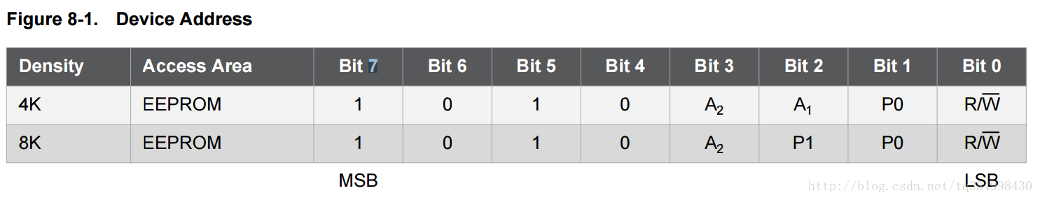
说得很清楚,AT24C08将器件地址(Device Addr)中的A1和A0位作为Page address,也就是说A1和A0是存储器的10位地址中的最高两位,我们再读写数据的时候要将地址的最高两位(page地址)放在这里。示例程序如下:
void IIC_Send(u8 device,u16 addr,u8 dat)
{
    IIC_Start();
    IIC_SendByte(device | (addr >> 8));
    IIC_Wait_Ack();
    IIC_SendByte((u8)addr);
    IIC_Wait_Ack();
    IIC_SendByte(dat);
    IIC_Wait_Ack();
    IIC_Stop();
}