A: IAR compiler interrupt function Description
Below that in the IAR, IAR must add at iostm8s105s6.h file, and finally there are the following in the file:
/ * ---------------------- -------------------------------------------------- -
* the Vector Interrupt a Numbers
* -------------------------------------------- * --------------------------- /
#define AWU_vector 0x03
#define SPI_TXE_vector 0x0C
#define SPI_RXNE_vector 0x0C
#define SPI_WKUP_vector 0x0C
#define SPI_CRCERR_vector 0x0C
# SPI_OVR_vector 0x0C the DEFINE
#define SPI_MODF_vector 0x0C
#define TIM1_OVR_UIF_vector 0x0D
#define TIM1_CAPCOM_BIF_vector 0x0D
#define TIM1_CAPCOM_TIF_vector 0x0D
#define TIM1_CAPCOM_CC1IF_vector 0x0E
#define TIM1_CAPCOM_CC2IF_vector 0x0E
#define TIM1_CAPCOM_CC3IF_vector 0x0E
#define TIM1_CAPCOM_CC4IF_vector 0x0E
#define TIM1_CAPCOM_COMIF_vector 0x0E
#define TIM2_OVR_UIF_vector 0x0F
#define TIM2_CAPCOM_CC1IF_vector 0x10
#define TIM2_CAPCOM_TIF_vector 0x10
#define TIM2_CAPCOM_CC2IF_vector 0x10
#define TIM2_CAPCOM_CC3IF_vector 0x10
#define UART1_T_TXE_vector 0x13
#define UART1_T_TC_vector 0x13
#define UART1_R_OR_vector 0x14
#define UART1_R_RXNE_vector 0x14
#define UART1_R_IDLE_vector 0x14
#define UART1_R_PE_vector 0x14
#define UART1_R_LBDF_vector 0x14
#define I2C_ADD10_vector 0x15
#define I2C_ADDR_vector 0x15
#define I2C_OVR_vector 0x15
#define I2C_STOPF_vector 0x15
#define I2C_BTF_vector 0x15
#define I2C_WUFH_vector 0x15
#define I2C_RXNE_vector 0x15
#define I2C_TXE_vector 0x15
#define I2C_BERR_vector 0x15
#define I2C_ARLO_vector 0x15
#define I2C_AF_vector 0x15
#define I2C_SB_vector 0x15
#define ADC1_AWS0_vector 0x18
#define ADC1_AWS1_vector 0x18
#define ADC1_AWS2_vector 0x18
#define ADC1_AWS3_vector 0x18
#define ADC1_AWS4_vector 0x18
#define ADC1_AWS5_vector 0x18
#define ADC1_AWS6_vector 0x18
#define ADC1_EOC_vector 0x18
#define ADC1_AWS8_vector 0x18
ADC1_AWS9_vector 0x18 #define
#define ADC1_AWDG_vector 0x18
#define ADC1_AWS7_vector 0x18
#define TIM4_OVR_UIF_vector 0x19
#define FLASH_EOP_vector 0x1A
#define FLASH_WR_PG_DIS_vector 0x1A
control the interrupt vector table, if used interrupt, the interrupt must write their own, such as TIM3 timer interrupt
#pragma the Vector = TIM3_OVR_UIF_vector
__interrupt TIM3_UPD_OVF_IRQHandler void (void)
{
TIM3_SR = 0X00; // Clear interrupt flag
}
Use keywords #pragma vector = point out this interrupt handler pointed to interrupt number, keyword __interrupt as a prefix function, that this is an interrupt handler.
Two: Interrupt Priority Description
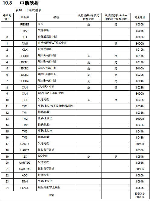
| 1 | 0 | 0 Ji ( main ) |
| 0 | 1 | Level 1 |
| 0 | 0 | Level 2 |
| 1 | 1 | 3 level (= disable software priority ) |
STM8 interrupt priority + software using hardware priority control method to control priority packets. Priority software to hardware priority. Hardware priority number determined by the vector, vector number, the higher the priority.
asm ( "sim"); // off global interrupt
asm ( "rim"); // open global interrupt
Define interrupt priority, and then open a total interruption.
Three: Introduction Timer 3 register
1, peripheral clock gating register (CLK_PCKENR1)
| Place 7: 0 | PCKEN1 [. 7: 0] : Peripheral Clock Enable written by software. Enable or disable F the MASTER is connected to the corresponding peripheral clock. See Table . 9 0 : Disable F the MASTER peripheral connections with 1 : Enable F the MASTER is connected to the peripheral |
Peripheral clock gating bit:
| Control bit | Peripherals |
| PCKEN17 | TIM1 |
| PCKEN16 | TIM3 |
| PCKEN15 | TIM2 |
| PCKEN14 | TIM4 |
| PCKEN13 | UART2 / 3 |
| PCKEN12 | UART1 |
| PCKEN11 | SPI |
| PCKEN10 | I2C |
Peripheral clock gating register 2 (CLK_PCKENR2)
| Place 7: 0 | PCKEN2 [. 7: 0] : Peripheral Clock Enable written by software. Enable or disable F the MASTER is connected to the corresponding peripheral clock. See Table 10 0 : Disable F the MASTER peripheral connections with 1 : Enable F the MASTER is connected to the peripheral |
Peripheral Clock Gating bit
| Control bit | Peripherals |
| PCKEN27 | CAN |
| PCKEN26 | Reserved |
| PCKEN25 | Reserved |
| PCKEN24 | Reserved |
| PCKEN23 | ADC |
| PCKEN22 | Well |
| PCKEN21 | Reserved |
| PCKEN20 | Reserved |
2, capture / compare mode register 1 (TIMx_CCMR1)
Channel configured as output:
Channel configured as input:

3, the capture / comparison mode register 2 (TIMx_CCMR2)
4, capture / compare enable register 1 (TIMx_CCER1)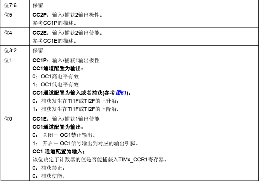
5, capture / compare enable register 2 (TIMx_CCER2)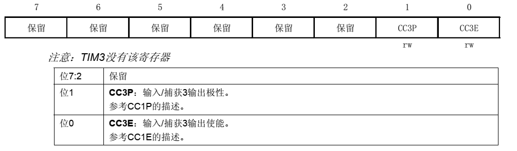
6, prescaler (TIMx_PSCR)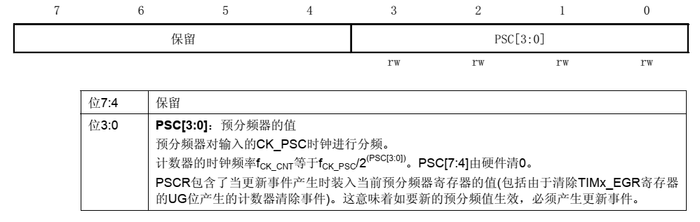
7,自动装载寄存器高位(TIMx_ARRH) ,自动装载寄存器低位(TIMx_ARRL) :保存自动装载值
8,捕获/比较寄存器 1 高位(TIMx_CCR1H) ,捕获/比较寄存器 1 低位(TIMx_CCR1L) :保存通道1捕获、比较的值,其余通道变序号即可
9,计数器高位(TIMx_CNTRH) ,计数器低位(TIMx_CNTRL) :保存计数器值
10,控制寄存器1(TIMx_CR1) 
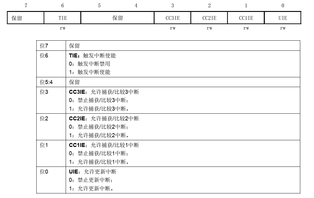
11,中断使能寄存器(TIMx_IER)
12,状态寄存器 1(TIMx_SR1) 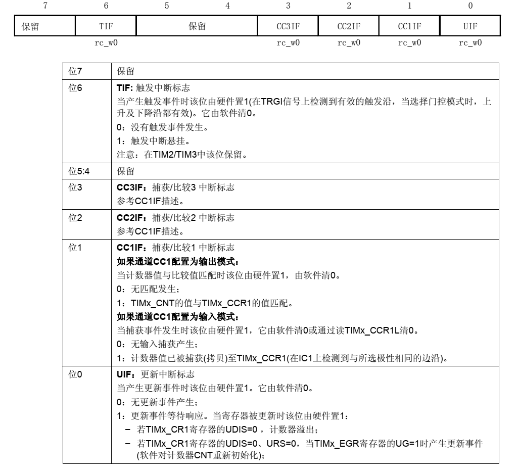
13,状态寄存器 2(TIMx_SR2) 
四:步骤
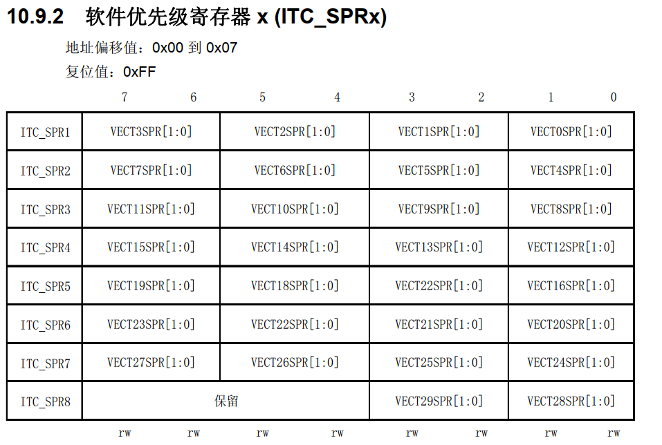
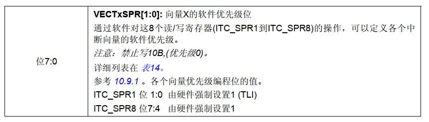
1,定时器3溢出中断软件优先级为级别1(寄存器ITC_SPR4)
2,开全局中断
3,开启定时器3外设时钟(寄存器CLK_PCKENR1)
4,设置定时器3一通道(PD2)pwm模式1,输出比较1预装载使能,CC1通道被配置为输出(寄存器TIM3_CCMR1)
5,OC1低电平有效,开启- OC1信号输出到对应的输出引脚(寄存器TIM3_CCER1)
6,始化时钟分频器为1,即不分频(寄存器TIM3_PSCR)
7,初始化自动装载寄存器,决定PWM 方波的频率(寄存器TIM3_ARRH , TIM3_ARRL)
8,初始化比较寄存器,决定PWM 方波的占空比(寄存器 TIM3_CCR1H ,TIM3_CCR1L )
9,设定定时器计数器的值,可要可不要(寄存器 TIM3_CNTRH=0x00,TIM3_CNTRL)
10,预装载不使能,非单脉冲模式,所有更新事件都会发送中断请求,正常产生更新事件,计数器不使能(寄存器TIM3_CR1)
11,允许更新中断(寄存器TIM3_IER)
12,开启定时器(寄存器 TIM3_CR1)
13,编写中断处理函数即可,记得要清除中断标志位。
五:完整代码
#include "iostm8s105s6.h"


void delay(unsigned int t);


void main()
{
  if(CLK_CMSR!=0xB4)//判断当前时钟,如果不是HSE则自动切换成HSE
  {
    CLK_SWCR|=0x02;//SWEN置1,使能切换
    CLK_SWR=0xB4;//目标时钟源为HSE外部晶振
    while((CLK_SWCR&0x08)==0);//等待,直到切换成功,SWIF被置位
    CLK_SWCR=0;//清除标志位
  }


  PG_DDR=0X01;//配置PG0为输出
  PG_CR1=0X01;//配置PG0为推挽输出
  PG_CR2=0X00;//输出速率=2MHz

  PD_DDR |= 0X04;             //设置PD2端口为输出模式
  PD_CR1 |= 0X04;             //设置PD2端口为推挽输出模式
  PD_CR2 &= 0XFD;

  ITC_SPR4=0X40;//定时器3溢出中断软件优先级为级别1
  asm("rim");//开全局中断

  CLK_PCKENR1|=0x40;//开启定时器3外设时钟
  TIM3_CCMR1 =0X68;   //设置定时器3一通道(PD2)pwm模式1,输出比较1预装载使能,CC1通道被配置为输出
  TIM3_CCER1 = 0x03;     //OC1低电平有效,开启- OC1信号输出到对应的输出引脚。
  TIM3_PSCR = 0X00; //初始化时钟分频器为1,即不分频

  //初始化自动装载寄存器,决定PWM 方波的频率
  TIM3_ARRH = 0X06;
  TIM3_ARRL = 0X40;

  //初始化比较寄存器,决定PWM 方波的占空比
  TIM3_CCR1H =0X03;
  TIM3_CCR1L =0X20;

  TIM3_CNTRH=0x00;//定时器计数器的值
  TIM3_CNTRL=0x00;

  TIM3_CR1=0x00;//预装载不使能,非单脉冲模式,所有更新事件都会发送中断请求,正常产生更新事件,计数器不使能
  TIM3_IER=0X01;//允许更新中断
  TIM3_CR1|=0x01;// 开启定时器

  while(1)
  {
    delay(50000);
  }
}

void delay(unsigned int t)
{
  while(t--);
}
#pragma vector=TIM3_OVR_UIF_vector

__interrupt void TIM3_UPD_OVF_IRQHandler (void)

{
  static int w=0;
  TIM3_SR1&=~0X01;//清除中断标志位

  w++;
  if(w<3000)
  {
      PG_ODR|=0X01;//小灯亮
  }
  else
  {
      PG_ODR&=0XFE;//小灯灭

  }
  if(w==6000)
  {
     w=0;
  }
}