[STM32] HAL library UART serial communication configuration with check bit to avoid pitfalls
Article directory
UART protocol
UART can complete the sending of data through one line
The other line can complete the receiving of data
So there are two lines in total TX RX
UART is low when idle
The clock cycle is determined by the baud rate, usually 115200bit/s
The UART protocol consists of four parts:
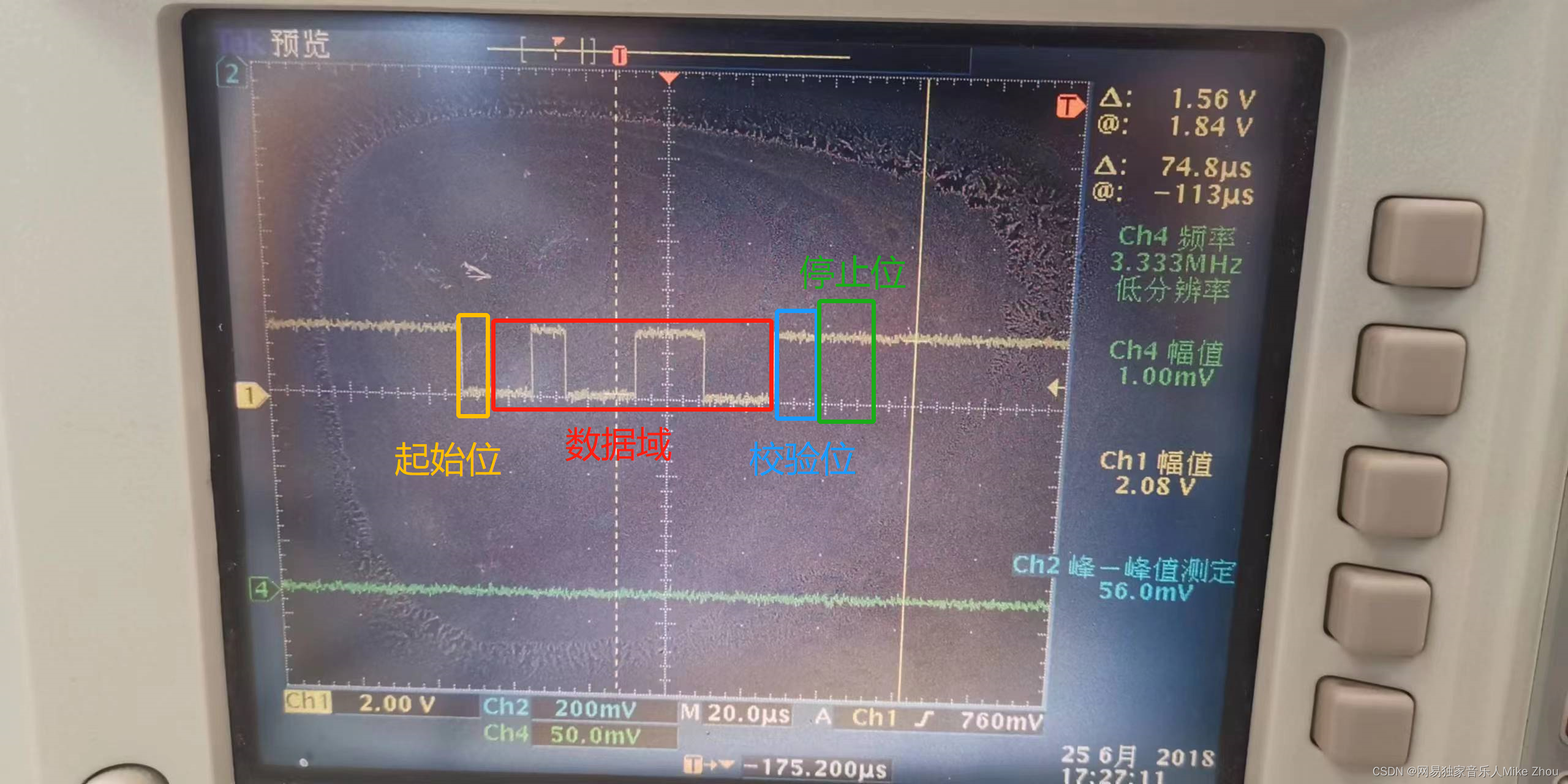
Start bit: Fixed low power Flat 1 clock cycle
Data field: usually 8 bit length LSB first
Parity bit: odd parity (odd) and even parity (even) It can also be none (none), usually no check bit
Stop bit: Fixed high level can be 0.5 1 1.5 2 clock cycles, usually 1
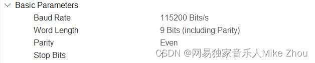
For example, the data field length is 8, the stop bit is 1, and there is no parity bit. Pass a 0x32
The order of sending data is:
0 0100 1100 1
Check Digit
The check digit is used to calculate the number of 1's in the previous data field
Odd parity: ensure that the number of 1's in the data field + check digit is an odd number a>
Even parity: ensure that the number of 1's in the data field + parity bit is an even number
In the above example, if even parity is added, the check digit is 1 (the first three 1s are so a 1 must be added to ensure it is an even number), so the whole becomes:
0 0100 1100 1 1
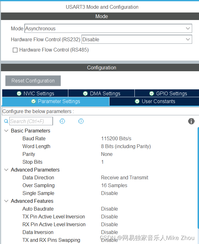
HAL library configuration
The default configuration of the HAL library is as follows:
Send function:
HAL_UART_Transmit
Receive function:
HAL_UART_Receive
Usually we use interrupts to receive
HAL_UART_Receive_IT
Avoiding bugs in serial port configuration with check digits
In the even parity configuration, I configured it like this:
Finally, I found that the waveform was like this (sending 0x32)
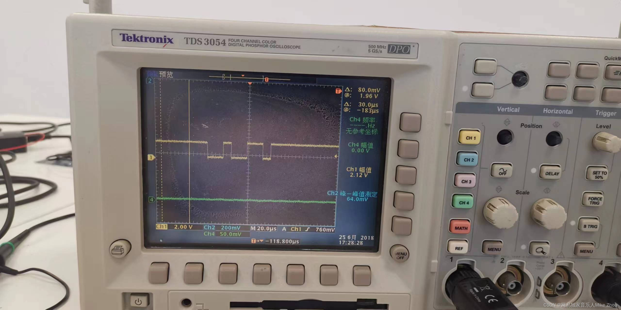
But if I don't set the check digit, it's normal
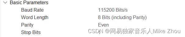
After debugging, I found that the word length used in the HAL library refers to the length of the data field + check digit, so if I configure it as above, the data field will only have 7 bits
If you want to send 8-bit data field and even parity data, you should configure it as follows: (that is, the word length should be one more bit)
The waveform also returns to normal:

Appendix: Cortex-M architecture SysTick system timer precise delay and MCU bit band operation
SysTick system timer precise delay
delay function
SysTick->The value in LOAD is the count value
The calculation method is the operating frequency value/frequency division value
For example, the operating frequency/1000 then The period is 1ms
Take ADuCM4050 as an example:
#include "ADuCM4050.h"

void delay_ms(unsigned int ms)
{


	SysTick->LOAD = 26000000/1000-1; // Count from 255 to 0 (256 cycles)  载入计数值 定时器从这个值开始计数
	SysTick->VAL = 0; // Clear current value as well as count flag  清空计数值到达0后的标记
	SysTick->CTRL = 5; // Enable SysTick timer with processor clock  使能52MHz的系统定时器
	while(ms--)
	{


		while ((SysTick->CTRL & 0x00010000)==0);// Wait until count flag is set  等待
	}
	SysTick->CTRL = 0; // Disable SysTick  关闭系统定时器
}
void delay_us(unsigned int us)
{


	SysTick->LOAD = 26000000/1000/1000-1; // Count from 255 to 0 (256 cycles)  载入计数值 定时器从这个值开始计数
	SysTick->VAL = 0; // Clear current value as well as count flag  清空计数值到达0后的标记
	SysTick->CTRL = 5; // Enable SysTick timer with processor clock  使能52MHz的系统定时器
	while(us--)
	{


		while ((SysTick->CTRL & 0x00010000)==0);// Wait until count flag is set  等待
	}
	SysTick->CTRL = 0; // Disable SysTick  关闭系统定时器
}
The 52000000 represents the system timer frequency of the chip. The 32 series is generally twice the external timer frequency.
Cortex-M architecture SysTick system timer blocking and non-blocking delay
blocking delay
The first is the most commonly used blocking delay
void delay_ms(unsigned int ms)
{


	SysTick->LOAD = 50000000/1000-1; // Count from 255 to 0 (256 cycles)  载入计数值 定时器从这个值开始计数
	SysTick->VAL = 0; // Clear current value as well as count flag  清空计数值到达0后的标记
	SysTick->CTRL = 5; // Enable SysTick timer with processor clock  使能26MHz的系统定时器
	while(ms--)
	{


		while ((SysTick->CTRL & 0x00010000)==0);// Wait until count flag is set  等待
	}
	SysTick->CTRL = 0; // Disable SysTick  关闭系统定时器
}
void delay_us(unsigned int us)
{


	SysTick->LOAD = 50000000/1000/1000-1; // Count from 255 to 0 (256 cycles)  载入计数值 定时器从这个值开始计数
	SysTick->VAL = 0; // Clear current value as well as count flag  清空计数值到达0后的标记
	SysTick->CTRL = 5; // Enable SysTick timer with processor clock  使能26MHz的系统定时器
	while(us--)
	{


		while ((SysTick->CTRL & 0x00010000)==0);// Wait until count flag is set  等待
	}
	SysTick->CTRL = 0; // Disable SysTick  关闭系统定时器
}
50000000 represents the operating frequency
After dividing the frequency, you can get different delay times
and so on
Then it can be written as: without two nested while loops:
void delay_ms(unsigned int ms)
{


	SysTick->LOAD = 50000000/1000*ms-1; // Count from 255 to 0 (256 cycles)  载入计数值 定时器从这个值开始计数
	SysTick->VAL = 0; // Clear current value as well as count flag  清空计数值到达0后的标记
	SysTick->CTRL = 5; // Enable SysTick timer with processor clock  使能26MHz的系统定时器

	while ((SysTick->CTRL & 0x00010000)==0);// Wait until count flag is set  等待

	SysTick->CTRL = 0; // Disable SysTick  关闭系统定时器
}
void delay_us(unsigned int us)
{


	SysTick->LOAD = 50000000/1000/1000*us-1; // Count from 255 to 0 (256 cycles)  载入计数值 定时器从这个值开始计数
	SysTick->VAL = 0; // Clear current value as well as count flag  清空计数值到达0后的标记
	SysTick->CTRL = 5; // Enable SysTick timer with processor clock  使能26MHz的系统定时器

	while ((SysTick->CTRL & 0x00010000)==0);// Wait until count flag is set  等待

	SysTick->CTRL = 0; // Disable SysTick  关闭系统定时器
}
But this way of writing has a drawback
That is, after inputting ms, the maximum timing must not exceed the count value, that is, it cannot exceed the maximum value of LOAD, otherwise it will not work normally after overflow. work
And if the maximum size of LOAD is 32 bits, that is 4294967295
If the crystal oscillator is 50M, the count value of 50M is 1s and the count value of 4294967295 is about 85s.
Fixed maximum timing time is 85s
But using nested while, the maximum supported timing is 4294967295*85s.
non-blocking delay
If non-blocking is used, just rewrite the second method directly:
void delay_ms(unsigned int ms)
{


	SysTick->LOAD = 50000000/1000*ms-1; // Count from 255 to 0 (256 cycles)  载入计数值 定时器从这个值开始计数
	SysTick->VAL = 0; // Clear current value as well as count flag  清空计数值到达0后的标记
	SysTick->CTRL = 5; // Enable SysTick timer with processor clock  使能26MHz的系统定时器

	//while ((SysTick->CTRL & 0x00010000)==0);// Wait until count flag is set  等待

	//SysTick->CTRL = 0; // Disable SysTick  关闭系统定时器
}
void delay_us(unsigned int us)
{


	SysTick->LOAD = 50000000/1000/1000*us-1; // Count from 255 to 0 (256 cycles)  载入计数值 定时器从这个值开始计数
	SysTick->VAL = 0; // Clear current value as well as count flag  清空计数值到达0后的标记
	SysTick->CTRL = 5; // Enable SysTick timer with processor clock  使能26MHz的系统定时器

	//while ((SysTick->CTRL & 0x00010000)==0);// Wait until count flag is set  等待

	//SysTick->CTRL = 0; // Disable SysTick  关闭系统定时器
}
Remove the wait and close timer statements
Add judgment when using it to become blocking:
delay_ms(500);
while ((SysTick->CTRL & 0x00010000)==0);
SysTick->CTRL = 0;
In a non-blocking state, you can submit the timer, do other things, and then wait again.
However, there is another drawback to this, that is, the timer will automatically reload. Maybe after doing other things, the timer will run out and you will have to wait 85 seconds to stop.
Therefore, non-blocking delay functions can be written through internal timers.
Basically, the internal timer of every MCU can be configured with automatic reloading and other functions. There is a lot of information online, so I won’t elaborate on it here.
Bitband operations
bitband code
The output address of the M3 and M4 architecture microcontroller is port address +20 and the input is +16
The output port address of the M0 architecture microcontroller is port address +12 and the input is +8
Taking ADuCM4050 as the column:
Bitband macro definition
#ifndef __GPIO_H__
#define __GPIO_H__
#include "ADuCM4050.h"
#include "adi_gpio.h"

#define BITBAND(addr, bitnum) ((addr & 0xF0000000)+0x2000000+((addr &0xFFFFF)<<5)+(bitnum<<2))
#define MEM_ADDR(addr)  *((volatile unsigned long  *)(addr))
#define BIT_ADDR(addr, bitnum)   MEM_ADDR(BITBAND(addr, bitnum))

#define GPIO0_ODR_Addr    (ADI_GPIO0_BASE+20) //0x40020014
#define GPIO0_IDR_Addr    (ADI_GPIO0_BASE+16) //0x40020010

#define GPIO1_ODR_Addr    (ADI_GPIO1_BASE+20) //0x40020054
#define GPIO1_IDR_Addr    (ADI_GPIO1_BASE+16) //0x40020050

#define GPIO2_ODR_Addr    (ADI_GPIO2_BASE+20) //0x40020094
#define GPIO2_IDR_Addr    (ADI_GPIO2_BASE+16) //0x40020090

#define GPIO3_ODR_Addr    (ADI_GPIO3_BASE+20) //0x400200D4
#define GPIO3_IDR_Addr    (ADI_GPIO3_BASE+16) //0x400200D0

#define P0_O(n)   	BIT_ADDR(GPIO0_ODR_Addr,n)  //输出
#define P0_I(n)    	BIT_ADDR(GPIO0_IDR_Addr,n)  //输入

#define P1_O(n)   	BIT_ADDR(GPIO1_ODR_Addr,n)  //输出
#define P1_I(n)    	BIT_ADDR(GPIO1_IDR_Addr,n)  //输入

#define P2_O(n)   	BIT_ADDR(GPIO2_ODR_Addr,n)  //输出
#define P2_I(n)    	BIT_ADDR(GPIO2_IDR_Addr,n)  //输入

#define P3_O(n)   	BIT_ADDR(GPIO3_ODR_Addr,n)  //输出
#define P3_I(n)    	BIT_ADDR(GPIO3_IDR_Addr,n)  //输入

#define Port0			(ADI_GPIO_PORT0)
#define Port1			(ADI_GPIO_PORT1)
#define Port2			(ADI_GPIO_PORT2)
#define Port3			(ADI_GPIO_PORT3)

#define Pin0			(ADI_GPIO_PIN_0)
#define Pin1			(ADI_GPIO_PIN_1)
#define Pin2			(ADI_GPIO_PIN_2)
#define Pin3			(ADI_GPIO_PIN_3)
#define Pin4			(ADI_GPIO_PIN_4)
#define Pin5			(ADI_GPIO_PIN_5)
#define Pin6			(ADI_GPIO_PIN_6)
#define Pin7			(ADI_GPIO_PIN_7)
#define Pin8			(ADI_GPIO_PIN_8)
#define Pin9			(ADI_GPIO_PIN_9)
#define Pin10			(ADI_GPIO_PIN_10)
#define Pin11			(ADI_GPIO_PIN_11)
#define Pin12			(ADI_GPIO_PIN_12)
#define Pin13			(ADI_GPIO_PIN_13)
#define Pin14			(ADI_GPIO_PIN_14)
#define Pin15			(ADI_GPIO_PIN_15)

void GPIO_OUT(unsigned int port,unsigned int pin,unsigned int flag);
void GPIO_BUS_OUT(unsigned int port,unsigned int num);

void P0_BUS_O(unsigned int num);
unsigned int P0_BUS_I(void);

void P1_BUS_O(unsigned int num);
unsigned int P1_BUS_I(void);

void P2_BUS_O(unsigned int num);
unsigned int P2_BUS_I(void);

void P3_BUS_O(unsigned int num);
unsigned int P3_BUS_I(void);

#endif
bus function
#include "ADuCM4050.h"
#include "adi_gpio.h"
#include "GPIO.h"

void GPIO_OUT(unsigned int port,unsigned int pin,unsigned int flag)
{


	switch(port)
	{


		case 0:{


			switch(pin)
			{


				case 0:if(flag==1){

    adi_gpio_SetHigh((ADI_GPIO_PORT0),(ADI_GPIO_PIN_0));}else{

    adi_gpio_SetLow((ADI_GPIO_PORT0),(ADI_GPIO_PIN_0));};break;
				case 1:if(flag==1){

    adi_gpio_SetHigh((ADI_GPIO_PORT0),(ADI_GPIO_PIN_1));}else{

    adi_gpio_SetLow((ADI_GPIO_PORT0),(ADI_GPIO_PIN_1));};break;
				case 2:if(flag==1){

    adi_gpio_SetHigh((ADI_GPIO_PORT0),(ADI_GPIO_PIN_2));}else{

    adi_gpio_SetLow((ADI_GPIO_PORT0),(ADI_GPIO_PIN_2));};break;
				case 3:if(flag==1){

    adi_gpio_SetHigh((ADI_GPIO_PORT0),(ADI_GPIO_PIN_3));}else{

    adi_gpio_SetLow((ADI_GPIO_PORT0),(ADI_GPIO_PIN_3));};break;
				case 4:if(flag==1){

    adi_gpio_SetHigh((ADI_GPIO_PORT0),(ADI_GPIO_PIN_4));}else{

    adi_gpio_SetLow((ADI_GPIO_PORT0),(ADI_GPIO_PIN_4));};break;
				case 5:if(flag==1){

    adi_gpio_SetHigh((ADI_GPIO_PORT0),(ADI_GPIO_PIN_5));}else{

    adi_gpio_SetLow((ADI_GPIO_PORT0),(ADI_GPIO_PIN_5));};break;
				case 6:if(flag==1){

    adi_gpio_SetHigh((ADI_GPIO_PORT0),(ADI_GPIO_PIN_6));}else{

    adi_gpio_SetLow((ADI_GPIO_PORT0),(ADI_GPIO_PIN_6));};break;
				case 7:if(flag==1){

    adi_gpio_SetHigh((ADI_GPIO_PORT0),(ADI_GPIO_PIN_7));}else{

    adi_gpio_SetLow((ADI_GPIO_PORT0),(ADI_GPIO_PIN_7));};break;
				case 8:if(flag==1){

    adi_gpio_SetHigh((ADI_GPIO_PORT0),(ADI_GPIO_PIN_8));}else{

    adi_gpio_SetLow((ADI_GPIO_PORT0),(ADI_GPIO_PIN_8));};break;
				case 9:if(flag==1){

    adi_gpio_SetHigh((ADI_GPIO_PORT0),(ADI_GPIO_PIN_9));}else{

    adi_gpio_SetLow((ADI_GPIO_PORT0),(ADI_GPIO_PIN_9));};break;
				case 10:if(flag==1){

    adi_gpio_SetHigh((ADI_GPIO_PORT0),(ADI_GPIO_PIN_10));}else{

    adi_gpio_SetLow((ADI_GPIO_PORT0),(ADI_GPIO_PIN_10));};break;
				case 11:if(flag==1){

    adi_gpio_SetHigh((ADI_GPIO_PORT0),(ADI_GPIO_PIN_11));}else{

    adi_gpio_SetLow((ADI_GPIO_PORT0),(ADI_GPIO_PIN_11));};break;
				case 12:if(flag==1){

    adi_gpio_SetHigh((ADI_GPIO_PORT0),(ADI_GPIO_PIN_12));}else{

    adi_gpio_SetLow((ADI_GPIO_PORT0),(ADI_GPIO_PIN_12));};break;
				case 13:if(flag==1){

    adi_gpio_SetHigh((ADI_GPIO_PORT0),(ADI_GPIO_PIN_13));}else{

    adi_gpio_SetLow((ADI_GPIO_PORT0),(ADI_GPIO_PIN_13));};break;
				case 14:if(flag==1){

    adi_gpio_SetHigh((ADI_GPIO_PORT0),(ADI_GPIO_PIN_14));}else{

    adi_gpio_SetLow((ADI_GPIO_PORT0),(ADI_GPIO_PIN_14));};break;
				case 15:if(flag==1){

    adi_gpio_SetHigh((ADI_GPIO_PORT0),(ADI_GPIO_PIN_15));}else{

    adi_gpio_SetLow((ADI_GPIO_PORT0),(ADI_GPIO_PIN_15));};break;
				default:pin=0;break;
			}
		}break;

		case 1:{


			switch(pin)
			{


				case 0:if(flag==1){

    adi_gpio_SetHigh((ADI_GPIO_PORT1),(ADI_GPIO_PIN_0));}else{

    adi_gpio_SetLow((ADI_GPIO_PORT1),(ADI_GPIO_PIN_0));};break;
				case 1:if(flag==1){

    adi_gpio_SetHigh((ADI_GPIO_PORT1),(ADI_GPIO_PIN_1));}else{

    adi_gpio_SetLow((ADI_GPIO_PORT1),(ADI_GPIO_PIN_1));};break;
				case 2:if(flag==1){

    adi_gpio_SetHigh((ADI_GPIO_PORT1),(ADI_GPIO_PIN_2));}else{

    adi_gpio_SetLow((ADI_GPIO_PORT1),(ADI_GPIO_PIN_2));};break;
				case 3:if(flag==1){

    adi_gpio_SetHigh((ADI_GPIO_PORT1),(ADI_GPIO_PIN_3));}else{

    adi_gpio_SetLow((ADI_GPIO_PORT1),(ADI_GPIO_PIN_3));};break;
				case 4:if(flag==1){

    adi_gpio_SetHigh((ADI_GPIO_PORT1),(ADI_GPIO_PIN_4));}else{

    adi_gpio_SetLow((ADI_GPIO_PORT1),(ADI_GPIO_PIN_4));};break;
				case 5:if(flag==1){

    adi_gpio_SetHigh((ADI_GPIO_PORT1),(ADI_GPIO_PIN_5));}else{

    adi_gpio_SetLow((ADI_GPIO_PORT1),(ADI_GPIO_PIN_5));};break;
				case 6:if(flag==1){

    adi_gpio_SetHigh((ADI_GPIO_PORT1),(ADI_GPIO_PIN_6));}else{

    adi_gpio_SetLow((ADI_GPIO_PORT1),(ADI_GPIO_PIN_6));};break;
				case 7:if(flag==1){

    adi_gpio_SetHigh((ADI_GPIO_PORT1),(ADI_GPIO_PIN_7));}else{

    adi_gpio_SetLow((ADI_GPIO_PORT1),(ADI_GPIO_PIN_7));};break;
				case 8:if(flag==1){

    adi_gpio_SetHigh((ADI_GPIO_PORT1),(ADI_GPIO_PIN_8));}else{

    adi_gpio_SetLow((ADI_GPIO_PORT1),(ADI_GPIO_PIN_8));};break;
				case 9:if(flag==1){

    adi_gpio_SetHigh((ADI_GPIO_PORT1),(ADI_GPIO_PIN_9));}else{

    adi_gpio_SetLow((ADI_GPIO_PORT1),(ADI_GPIO_PIN_9));};break;
				case 10:if(flag==1){

    adi_gpio_SetHigh((ADI_GPIO_PORT1),(ADI_GPIO_PIN_10));}else{

    adi_gpio_SetLow((ADI_GPIO_PORT1),(ADI_GPIO_PIN_10));};break;
				case 11:if(flag==1){

    adi_gpio_SetHigh((ADI_GPIO_PORT1),(ADI_GPIO_PIN_11));}else{

    adi_gpio_SetLow((ADI_GPIO_PORT1),(ADI_GPIO_PIN_11));};break;
				case 12:if(flag==1){

    adi_gpio_SetHigh((ADI_GPIO_PORT1),(ADI_GPIO_PIN_12));}else{

    adi_gpio_SetLow((ADI_GPIO_PORT1),(ADI_GPIO_PIN_12));};break;
				case 13:if(flag==1){

    adi_gpio_SetHigh((ADI_GPIO_PORT1),(ADI_GPIO_PIN_13));}else{

    adi_gpio_SetLow((ADI_GPIO_PORT1),(ADI_GPIO_PIN_13));};break;
				case 14:if(flag==1){

    adi_gpio_SetHigh((ADI_GPIO_PORT1),(ADI_GPIO_PIN_14));}else{

    adi_gpio_SetLow((ADI_GPIO_PORT1),(ADI_GPIO_PIN_14));};break;
				case 15:if(flag==1){

    adi_gpio_SetHigh((ADI_GPIO_PORT1),(ADI_GPIO_PIN_15));}else{

    adi_gpio_SetLow((ADI_GPIO_PORT1),(ADI_GPIO_PIN_15));};break;
				default:pin=0;break;
			}
		}break;

		case 2:{


			switch(pin)
			{


				case 0:if(flag==1){

    adi_gpio_SetHigh((ADI_GPIO_PORT2),(ADI_GPIO_PIN_0));}else{

    adi_gpio_SetLow((ADI_GPIO_PORT2),(ADI_GPIO_PIN_0));};break;
				case 1:if(flag==1){

    adi_gpio_SetHigh((ADI_GPIO_PORT2),(ADI_GPIO_PIN_1));}else{

    adi_gpio_SetLow((ADI_GPIO_PORT2),(ADI_GPIO_PIN_1));};break;
				case 2:if(flag==1){

    adi_gpio_SetHigh((ADI_GPIO_PORT2),(ADI_GPIO_PIN_2));}else{

    adi_gpio_SetLow((ADI_GPIO_PORT2),(ADI_GPIO_PIN_2));};break;
				case 3:if(flag==1){

    adi_gpio_SetHigh((ADI_GPIO_PORT2),(ADI_GPIO_PIN_3));}else{

    adi_gpio_SetLow((ADI_GPIO_PORT2),(ADI_GPIO_PIN_3));};break;
				case 4:if(flag==1){

    adi_gpio_SetHigh((ADI_GPIO_PORT2),(ADI_GPIO_PIN_4));}else{

    adi_gpio_SetLow((ADI_GPIO_PORT2),(ADI_GPIO_PIN_4));};break;
				case 5:if(flag==1){

    adi_gpio_SetHigh((ADI_GPIO_PORT2),(ADI_GPIO_PIN_5));}else{

    adi_gpio_SetLow((ADI_GPIO_PORT2),(ADI_GPIO_PIN_5));};break;
				case 6:if(flag==1){

    adi_gpio_SetHigh((ADI_GPIO_PORT2),(ADI_GPIO_PIN_6));}else{

    adi_gpio_SetLow((ADI_GPIO_PORT2),(ADI_GPIO_PIN_6));};break;
				case 7:if(flag==1){

    adi_gpio_SetHigh((ADI_GPIO_PORT2),(ADI_GPIO_PIN_7));}else{

    adi_gpio_SetLow((ADI_GPIO_PORT2),(ADI_GPIO_PIN_7));};break;
				case 8:if(flag==1){

    adi_gpio_SetHigh((ADI_GPIO_PORT2),(ADI_GPIO_PIN_8));}else{

    adi_gpio_SetLow((ADI_GPIO_PORT2),(ADI_GPIO_PIN_8));};break;
				case 9:if(flag==1){

    adi_gpio_SetHigh((ADI_GPIO_PORT2),(ADI_GPIO_PIN_9));}else{

    adi_gpio_SetLow((ADI_GPIO_PORT2),(ADI_GPIO_PIN_9));};break;
				case 10:if(flag==1){

    adi_gpio_SetHigh((ADI_GPIO_PORT2),(ADI_GPIO_PIN_10));}else{

    adi_gpio_SetLow((ADI_GPIO_PORT2),(ADI_GPIO_PIN_10));};break;
				case 11:if(flag==1){

    adi_gpio_SetHigh((ADI_GPIO_PORT2),(ADI_GPIO_PIN_11));}else{

    adi_gpio_SetLow((ADI_GPIO_PORT2),(ADI_GPIO_PIN_11));};break;
				case 12:if(flag==1){

    adi_gpio_SetHigh((ADI_GPIO_PORT2),(ADI_GPIO_PIN_12));}else{

    adi_gpio_SetLow((ADI_GPIO_PORT2),(ADI_GPIO_PIN_12));};break;
				case 13:if(flag==1){

    adi_gpio_SetHigh((ADI_GPIO_PORT2),(ADI_GPIO_PIN_13));}else{

    adi_gpio_SetLow((ADI_GPIO_PORT2),(ADI_GPIO_PIN_13));};break;
				case 14:if(flag==1){

    adi_gpio_SetHigh((ADI_GPIO_PORT2),(ADI_GPIO_PIN_14));}else{

    adi_gpio_SetLow((ADI_GPIO_PORT2),(ADI_GPIO_PIN_14));};break;
				case 15:if(flag==1){

    adi_gpio_SetHigh((ADI_GPIO_PORT2),(ADI_GPIO_PIN_15));}else{

    adi_gpio_SetLow((ADI_GPIO_PORT2),(ADI_GPIO_PIN_15));};break;
				default:pin=0;break;
			}
		}break;

		case 3:{


			switch(pin)
			{


				case 0:if(flag==1){

    adi_gpio_SetHigh((ADI_GPIO_PORT3),(ADI_GPIO_PIN_0));}else{

    adi_gpio_SetLow((ADI_GPIO_PORT3),(ADI_GPIO_PIN_0));};break;
				case 1:if(flag==1){

    adi_gpio_SetHigh((ADI_GPIO_PORT3),(ADI_GPIO_PIN_1));}else{

    adi_gpio_SetLow((ADI_GPIO_PORT3),(ADI_GPIO_PIN_1));};break;
				case 2:if(flag==1){

    adi_gpio_SetHigh((ADI_GPIO_PORT3),(ADI_GPIO_PIN_2));}else{

    adi_gpio_SetLow((ADI_GPIO_PORT3),(ADI_GPIO_PIN_2));};break;
				case 3:if(flag==1){

    adi_gpio_SetHigh((ADI_GPIO_PORT3),(ADI_GPIO_PIN_3));}else{

    adi_gpio_SetLow((ADI_GPIO_PORT3),(ADI_GPIO_PIN_3));};break;
				case 4:if(flag==1){

    adi_gpio_SetHigh((ADI_GPIO_PORT3),(ADI_GPIO_PIN_4));}else{

    adi_gpio_SetLow((ADI_GPIO_PORT3),(ADI_GPIO_PIN_4));};break;
				case 5:if(flag==1){

    adi_gpio_SetHigh((ADI_GPIO_PORT3),(ADI_GPIO_PIN_5));}else{

    adi_gpio_SetLow((ADI_GPIO_PORT3),(ADI_GPIO_PIN_5));};break;
				case 6:if(flag==1){

    adi_gpio_SetHigh((ADI_GPIO_PORT3),(ADI_GPIO_PIN_6));}else{

    adi_gpio_SetLow((ADI_GPIO_PORT3),(ADI_GPIO_PIN_6));};break;
				case 7:if(flag==1){

    adi_gpio_SetHigh((ADI_GPIO_PORT3),(ADI_GPIO_PIN_7));}else{

    adi_gpio_SetLow((ADI_GPIO_PORT3),(ADI_GPIO_PIN_7));};break;
				case 8:if(flag==1){

    adi_gpio_SetHigh((ADI_GPIO_PORT3),(ADI_GPIO_PIN_8));}else{

    adi_gpio_SetLow((ADI_GPIO_PORT3),(ADI_GPIO_PIN_8));};break;
				case 9:if(flag==1){

    adi_gpio_SetHigh((ADI_GPIO_PORT3),(ADI_GPIO_PIN_9));}else{

    adi_gpio_SetLow((ADI_GPIO_PORT3),(ADI_GPIO_PIN_9));};break;
				case 10:if(flag==1){

    adi_gpio_SetHigh((ADI_GPIO_PORT3),(ADI_GPIO_PIN_10));}else{

    adi_gpio_SetLow((ADI_GPIO_PORT3),(ADI_GPIO_PIN_10));};break;
				case 11:if(flag==1){

    adi_gpio_SetHigh((ADI_GPIO_PORT3),(ADI_GPIO_PIN_11));}else{

    adi_gpio_SetLow((ADI_GPIO_PORT3),(ADI_GPIO_PIN_11));};break;
				case 12:if(flag==1){

    adi_gpio_SetHigh((ADI_GPIO_PORT3),(ADI_GPIO_PIN_12));}else{

    adi_gpio_SetLow((ADI_GPIO_PORT3),(ADI_GPIO_PIN_12));};break;
				case 13:if(flag==1){

    adi_gpio_SetHigh((ADI_GPIO_PORT3),(ADI_GPIO_PIN_13));}else{

    adi_gpio_SetLow((ADI_GPIO_PORT3),(ADI_GPIO_PIN_13));};break;
				case 14:if(flag==1){

    adi_gpio_SetHigh((ADI_GPIO_PORT3),(ADI_GPIO_PIN_14));}else{

    adi_gpio_SetLow((ADI_GPIO_PORT3),(ADI_GPIO_PIN_14));};break;
				case 15:if(flag==1){

    adi_gpio_SetHigh((ADI_GPIO_PORT3),(ADI_GPIO_PIN_15));}else{

    adi_gpio_SetLow((ADI_GPIO_PORT3),(ADI_GPIO_PIN_15));};break;
				default:pin=0;break;
			}
		}break;

		default:port=0;break;
	}
}

void GPIO_BUS_OUT(unsigned int port,unsigned int num)  //num最大为0xffff
{


	int i;
	for(i=0;i<16;i++)
	{


		GPIO_OUT(port,i,(num>>i)&0x0001);
	}
}


void P0_BUS_O(unsigned int num)  //输入值num最大为0xFFFF
{


	int i;
	for(i=0;i<16;i++)
	{


		P0_O(i)=(num>>i)&0x0001;
	}
}
unsigned int P0_BUS_I(void)  //输出值num最大为0xFFFF
{


	unsigned int num;
	int i;
	for(i=0;i<16;i++)
	{


		num=num+(P0_I(i)<<i)&0xFFFF;
	}
	return num;
}

void P1_BUS_O(unsigned int num)  //输入值num最大为0xFFFF
{


	int i;
	for(i=0;i<16;i++)
	{


		P1_O(i)=(num>>i)&0x0001;
	}
}
unsigned int P1_BUS_I(void)  //输出值num最大为0xFFFF
{


	unsigned int num;
	int i;
	for(i=0;i<16;i++)
	{


		num=num+(P1_I(i)<<i)&0xFFFF;
	}
	return num;
}

void P2_BUS_O(unsigned int num)  //输入值num最大为0xFFFF
{


	int i;
	for(i=0;i<16;i++)
	{


		P2_O(i)=(num>>i)&0x0001;
	}
}
unsigned int P2_BUS_I(void)  //输出值num最大为0xFFFF
{


	unsigned int num;
	int i;
	for(i=0;i<16;i++)
	{


		num=num+(P2_I(i)<<i)&0xFFFF;
	}
	return num;
}

void P3_BUS_O(unsigned int num)  //输入值num最大为0xFFFF
{


	int i;
	for(i=0;i<16;i++)
	{


		P3_O(i)=(num>>i)&0x0001;
	}
}
unsigned int P3_BUS_I(void)  //输出值num最大为0xFFFF
{


	unsigned int num;
	int i;
	for(i=0;i<16;i++)
	{


		num=num+(P3_I(i)<<i)&0xFFFF;
	}
	return num;
}
1. Bit band operation theory and practice
The concept of bit band operation actually existed 30 years ago. It was CM3 that evolved this capability. The bit band operation here is a greatly enhanced version of the 8051 bit addressing area.
Bitband area: Address area that supports bitband operations
Bitband alias: Access to the alias address ultimately affects access to the bitband (note: there is an address mapping process in the middle)
Bitband operations are most useful for low-level programs that are hardware I/O intensive.
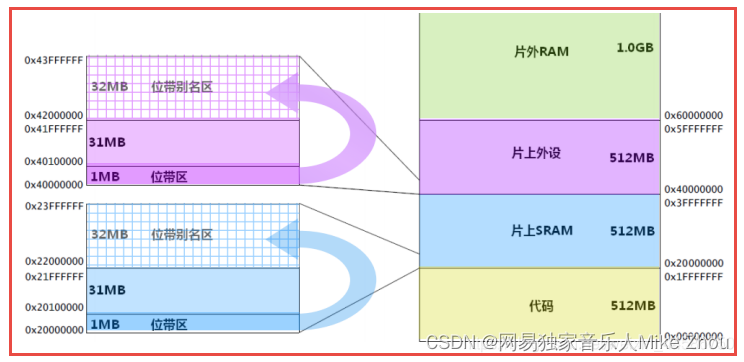
After supporting bit band operations, ordinary load/store instructions can be used to read and write single bits. In CM4, bitbanding is implemented in two zones. One of them is the lowest 1MB range of the SRAM area, and the second is the lowest 1MB range of the on-chip peripheral area. In addition to being used like ordinary RAM, the addresses in these two areas also have their own "bit band alias area", which expands each bit into a 32-bit word. When you access these words through the bitband alias area, you can access the original bits.
Bit operation means that you can read and write a bit individually, similar to the variable defined by sbit in 51. In stm32, the function of bit operation is realized by accessing the bit alias area
Bit strips are implemented in two places in STM32, one is SRAM and the other is on-chip peripherals.
(1) The bit band is essentially an address area (for example, each address bit corresponds to a register) mapped to another address area (each address bit corresponds to a register) bit), this area is called the bit band alias area, and each bit is expanded into a 32-bit word.
(2) The 4 bytes of the bit band area correspond to one bit of the actual register or memory area. Although it becomes larger to 4 bytes, only the lowest bit is actually valid (representing 0 or 1)
Only the bit band can be directly operated using = assignment. The bit band expands each bit in the register to 32 bits and maps it to the bit band. For example, the 0th bit of the 0x4002 0000 address is mapped to the 0 address of the bit band. Then its corresponding The bit band mapping address is 0x00 - 0x04, a total of 32 bits, but only the LSB is valid in bit band mode. When assigning a value, the LSB corresponding to the bit band area is assigned, and then the MCU goes to the corresponding bit in the register. If the register operation does not change The values on other bits can only be determined by &= or |=.
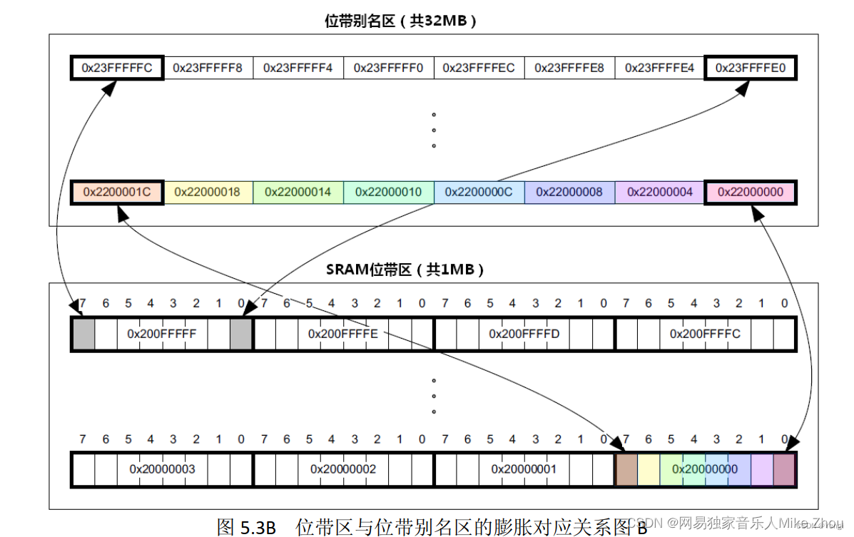
To set the second bit bit2 of the byte 0x2000 0000 to 1, the steps to use the bit band operation are:
1. Write 1 to the corresponding bit band alias area Mapping address (i.e. 0x22000008, because 1 bit corresponds to 4 bytes);
2. Read the value of 0x2000 0000 into the internal buffer (this step is completed by the kernel and is an atomic operation. No user operation is required);
3. Set bit2 to 1, and then write the value back to 0x2000 0000 (it is an atomic operation and does not require user operation).
For the access address corresponding to the GPIO pin, you can refer to the following formula
Register bit with alias = 0x42000000 + (register address-0x40000000) 32 + pin number4
For example: the starting address GPIOF_BASE for port F access
#define GPIOF ((GPIO_TypeDef *)GPIOF_BASE)
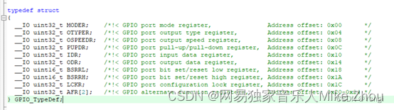
But fortunately, the official library has defined it for us. We only need to add cheap to the BASE address.
For example:
The address of the ODR register of GPIOF = GPIOF_BASE + 0x14
Register bit with alias = 0x42000000 + (register address-0x40000000)32 + pin number4
To set the PF9 pin:
uint32_t *PF9_BitBand =
*(uint32_t *)(0x42000000 + ((uint32_t )&GPIOF->ODR– 0x40000000) *32 + 9*4)
Encapsulate it:
#define PFout(x) *(volatile uint32_t *)(0x42000000 + ((uint32_t )&GPIOF->ODR – 0x40000000) *32 + x*4)
Now the common part can be encapsulated into a small definition:
#define BITBAND(addr, bitnum) ((addr & 0xF0000000)+0x2000000+((addr &0xFFFFF)<<5)+(bitnum<<2))
#define MEM_ADDR(addr)  *((volatile unsigned long  *)(addr))
#define BIT_ADDR(addr, bitnum)   MEM_ADDR(BITBAND(addr, bitnum))
Then the function to set the PF pin can be defined:
#define GPIOF_ODR_Addr    (GPIOF_BASE+20) //0x40021414
#define GPIOF_IDR_Addr    (GPIOF_BASE+16) //0x40021410

#define PF_O(n)   	BIT_ADDR(GPIOF_ODR_Addr,n)  //输出
#define PF_I(n)    	BIT_ADDR(GPIOF_IDR_Addr,n)  //输入
If PF9 is enabled for input and output:
PF_O(9)=1;  //输出高电平
uint8_t dat = PF_I(9);  //获取PF9引脚的值
Bus input and output:
void PF_BUS_O(unsigned int num)  //输入值num最大为0xFFFF
{


	int i;
	for(i=0;i<16;i++)
	{


		PF_O(i)=(num>>i)&0x0001;
	}
}
unsigned int PF_BUS_I(void)  //输出值num最大为0xFFFF
{


	unsigned int num;
	int i;
	for(i=0;i<16;i++)
	{


		num=num+(PF_I(i)<<i)&0xFFFF;
	}
	return num;
}
The following functions are available for STM32:
#ifndef __GPIO_H__
#define __GPIO_H__
#include "stm32l496xx.h"

#define BITBAND(addr, bitnum) ((addr & 0xF0000000)+0x2000000+((addr &0xFFFFF)<<5)+(bitnum<<2))
#define MEM_ADDR(addr)  *((volatile unsigned long  *)(addr))
#define BIT_ADDR(addr, bitnum)   MEM_ADDR(BITBAND(addr, bitnum))

#define GPIOA_ODR_Addr    (GPIOA_BASE+20) //0x40020014
#define GPIOB_ODR_Addr    (GPIOB_BASE+20) //0x40020414
#define GPIOC_ODR_Addr    (GPIOC_BASE+20) //0x40020814
#define GPIOD_ODR_Addr    (GPIOD_BASE+20) //0x40020C14
#define GPIOE_ODR_Addr    (GPIOE_BASE+20) //0x40021014
#define GPIOF_ODR_Addr    (GPIOF_BASE+20) //0x40021414
#define GPIOG_ODR_Addr    (GPIOG_BASE+20) //0x40021814
#define GPIOH_ODR_Addr    (GPIOH_BASE+20) //0x40021C14
#define GPIOI_ODR_Addr    (GPIOI_BASE+20) //0x40022014

#define GPIOA_IDR_Addr    (GPIOA_BASE+16) //0x40020010
#define GPIOB_IDR_Addr    (GPIOB_BASE+16) //0x40020410
#define GPIOC_IDR_Addr    (GPIOC_BASE+16) //0x40020810
#define GPIOD_IDR_Addr    (GPIOD_BASE+16) //0x40020C10
#define GPIOE_IDR_Addr    (GPIOE_BASE+16) //0x40021010
#define GPIOF_IDR_Addr    (GPIOF_BASE+16) //0x40021410
#define GPIOG_IDR_Addr    (GPIOG_BASE+16) //0x40021810
#define GPIOH_IDR_Addr    (GPIOH_BASE+16) //0x40021C10
#define GPIOI_IDR_Addr    (GPIOI_BASE+16) //0x40022010

#define PA_O(n)   	BIT_ADDR(GPIOA_ODR_Addr,n)  //输出
#define PA_I(n)    	BIT_ADDR(GPIOA_IDR_Addr,n)  //输入

#define PB_O(n)   	BIT_ADDR(GPIOB_ODR_Addr,n)  //输出
#define PB_I(n)    	BIT_ADDR(GPIOB_IDR_Addr,n)  //输入

#define PC_O(n)   	BIT_ADDR(GPIOC_ODR_Addr,n)  //输出
#define PC_I(n)    	BIT_ADDR(GPIOC_IDR_Addr,n)  //输入

#define PD_O(n)   	BIT_ADDR(GPIOD_ODR_Addr,n)  //输出
#define PD_I(n)    	BIT_ADDR(GPIOD_IDR_Addr,n)  //输入

#define PE_O(n)   	BIT_ADDR(GPIOE_ODR_Addr,n)  //输出
#define PE_I(n)    	BIT_ADDR(GPIOE_IDR_Addr,n)  //输入

#define PF_O(n)   	BIT_ADDR(GPIOF_ODR_Addr,n)  //输出
#define PF_I(n)    	BIT_ADDR(GPIOF_IDR_Addr,n)  //输入

#define PG_O(n)   	BIT_ADDR(GPIOG_ODR_Addr,n)  //输出
#define PG_I(n)    	BIT_ADDR(GPIOG_IDR_Addr,n)  //输入

#define PH_O(n)   	BIT_ADDR(GPIOH_ODR_Addr,n)  //输出
#define PH_I(n)    	BIT_ADDR(GPIOH_IDR_Addr,n)  //输入

#define PI_O(n)			BIT_ADDR(GPIOI_ODR_Addr,n)  //输出
#define PI_I(n)   	BIT_ADDR(GPIOI_IDR_Addr,n)  //输入

void PA_BUS_O(unsigned int num);
unsigned int PA_BUS_I(void);

void PB_BUS_O(unsigned int num);
unsigned int PB_BUS_I(void);

void PC_BUS_O(unsigned int num);
unsigned int PC_BUS_I(void);

void PD_BUS_O(unsigned int num);
unsigned int PD_BUS_I(void);

void PE_BUS_O(unsigned int num);
unsigned int PE_BUS_I(void);

void PF_BUS_O(unsigned int num);
unsigned int PF_BUS_I(void);

void PG_BUS_O(unsigned int num);
unsigned int PG_BUS_I(void);

void PH_BUS_O(unsigned int num);
unsigned int PH_BUS_I(void);

void PI_BUS_O(unsigned int num);
unsigned int PI_BUS_I(void);

#endif
#include "GPIO.h"

void PA_BUS_O(unsigned int num)  //输入值num最大为0xFFFF
{


	int i;
	for(i=0;i<16;i++)
	{


		PA_O(i)=(num>>i)&0x0001;
	}
}
unsigned int PA_BUS_I(void)  //输出值num最大为0xFFFF
{


	unsigned int num;
	int i;
	for(i=0;i<16;i++)
	{


		num=num+(PA_I(i)<<i)&0xFFFF;
	}
	return num;
}

void PB_BUS_O(unsigned int num)  //输入值num最大为0xFFFF
{


	int i;
	for(i=0;i<16;i++)
	{


		PB_O(i)=(num>>i)&0x0001;
	}
}
unsigned int PB_BUS_I(void)  //输出值num最大为0xFFFF
{


	unsigned int num;
	int i;
	for(i=0;i<16;i++)
	{


		num=num+(PB_I(i)<<i)&0xFFFF;
	}
	return num;
}

void PC_BUS_O(unsigned int num)  //输入值num最大为0xFFFF
{


	int i;
	for(i=0;i<16;i++)
	{


		PC_O(i)=(num>>i)&0x0001;
	}
}
unsigned int PC_BUS_I(void)  //输出值num最大为0xFFFF
{


	unsigned int num;
	int i;
	for(i=0;i<16;i++)
	{


		num=num+(PC_I(i)<<i)&0xFFFF;
	}
	return num;
}

void PD_BUS_O(unsigned int num)  //输入值num最大为0xFFFF
{


	int i;
	for(i=0;i<16;i++)
	{


		PD_O(i)=(num>>i)&0x0001;
	}
}
unsigned int PD_BUS_I(void)  //输出值num最大为0xFFFF
{


	unsigned int num;
	int i;
	for(i=0;i<16;i++)
	{


		num=num+(PD_I(i)<<i)&0xFFFF;
	}
	return num;
}

void PE_BUS_O(unsigned int num)  //输入值num最大为0xFFFF
{


	int i;
	for(i=0;i<16;i++)
	{


		PE_O(i)=(num>>i)&0x0001;
	}
}
unsigned int PE_BUS_I(void)  //输出值num最大为0xFFFF
{


	unsigned int num;
	int i;
	for(i=0;i<16;i++)
	{


		num=num+(PE_I(i)<<i)&0xFFFF;
	}
	return num;
}

void PF_BUS_O(unsigned int num)  //输入值num最大为0xFFFF
{


	int i;
	for(i=0;i<16;i++)
	{


		PF_O(i)=(num>>i)&0x0001;
	}
}
unsigned int PF_BUS_I(void)  //输出值num最大为0xFFFF
{


	unsigned int num;
	int i;
	for(i=0;i<16;i++)
	{


		num=num+(PF_I(i)<<i)&0xFFFF;
	}
	return num;
}

void PG_BUS_O(unsigned int num)  //输入值num最大为0xFFFF
{


	int i;
	for(i=0;i<16;i++)
	{


		PG_O(i)=(num>>i)&0x0001;
	}
}
unsigned int PG_BUS_I(void)  //输出值num最大为0xFFFF
{


	unsigned int num;
	int i;
	for(i=0;i<16;i++)
	{


		num=num+(PG_I(i)<<i)&0xFFFF;
	}
	return num;
}

void PH_BUS_O(unsigned int num)  //输入值num最大为0xFFFF
{


	int i;
	for(i=0;i<16;i++)
	{


		PH_O(i)=(num>>i)&0x0001;
	}
}
unsigned int PH_BUS_I(void)  //输出值num最大为0xFFFF
{


	unsigned int num;
	int i;
	for(i=0;i<16;i++)
	{


		num=num+(PH_I(i)<<i)&0xFFFF;
	}
	return num;
}

void PI_BUS_O(unsigned int num)  //输入值num最大为0xFFFF
{


	int i;
	for(i=0;i<16;i++)
	{


		PI_O(i)=(num>>i)&0x0001;
	}
}
unsigned int PI_BUS_I(void)  //输出值num最大为0xFFFF
{


	unsigned int num;
	int i;
	for(i=0;i<16;i++)
	{


		num=num+(PI_I(i)<<i)&0xFFFF;
	}
	return num;
}
2. How to determine whether the MCU peripherals support bit banding
According to the description in Chapter 6, Section 7 of "ARM Cortex-M3 and Cortex-M4 Authoritative Guide (3rd Edition)"
In other words, it is necessary to implement the bit banding of GPIO The operation must ensure that the GPIO is located in the first 1MB of the peripheral area
The first 1MB should be 0x4010. The bit band before 0000 is not a direct operation address but an operation address mapping. After the address mapping is operated, the MCU automatically Will modify the value of the corresponding register
The bit band area is only 1MB, so you can only change the registers 0x4000 0000 - 0x400F FFFF
For example, if the first address of the F4 series GPIO is 0x4002 0000, you can use the bit band to change it
The GPIO of STM32L476 does not work:
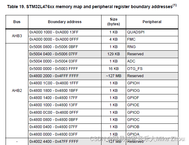
AHB2 cannot use bitbands
Both ABP and AHB1 can be used
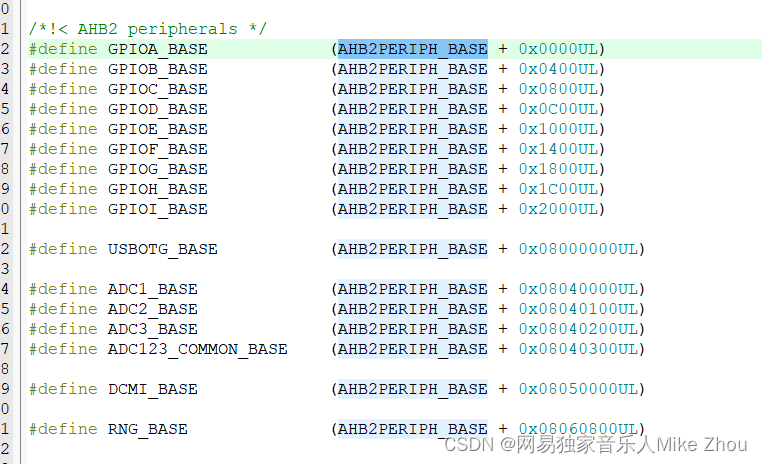
But the GPIO and ADC in the L476 register are both AHB2