一、前言
最近花费很多精力在算法仿真和实现上,外设接口的调试略有生疏。本文以FPGA控制OLED中的SPI接口为例,重新夯实下基础。重点内容为SPI时序的RTL设计以及AXI-Lite总线分析。当然做些项目时可以直接调用Xilinx提供的SPI IP核,这里仅出于练习的目的考虑。
二、接口时序分析
本项目用的OLED型号为UG-2832HSWEG04,核心控制器是SSD1306。该芯片支持并口、I2C以及SPI接口,这里采用4线SPI作为数据总线。4线SPI接口包括:
SCLK:串行时钟,SSD1306上升沿采集数据
SDIN:串行数据输入,数据顺序为MSB
D/C:数据命令控制,高电平为数据,低电平为控制命令
CS:片选信号,低电平有效
时序图如下:
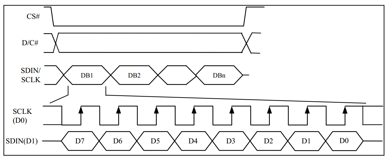
片选信号有效期间,每第8个时钟周期上升沿时刻,控制芯片会采样D/C并同时将进入的一字节数据写入到显示缓存GDDRAM或控制寄存器中。
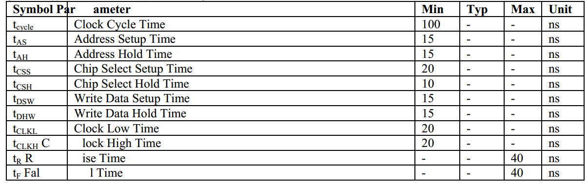
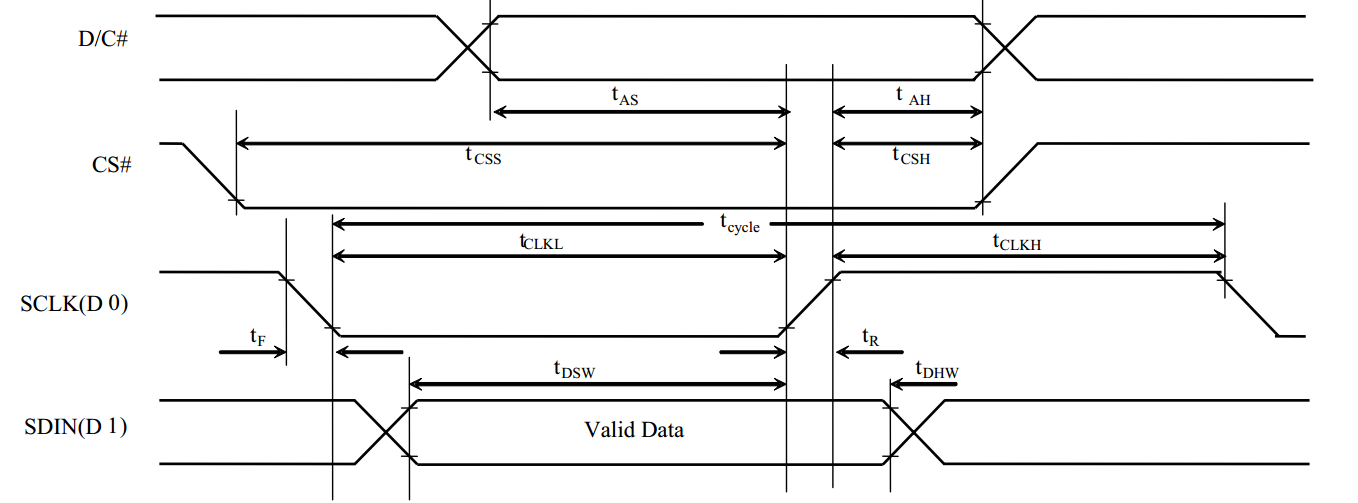
根据datasheet中的AC Characteristics中参数,选择SPI串行时钟周期为200ns,占空比为50%以保证足够的时序裕量。此时传输速率为:5MHZ/8 = 625KHZ。
三、SPI接口模块设计
根据上述分析,很容易可以设计出用于传输数据或命令的SPI时序接口模块。接口定义如下:
用户侧:clk rst_n com din busy,依次是系统时钟,复位,指令信号(1为发送控制信息,2则发送数据),待传输字节以及忙等待指示。
外设侧:SCLK SDIN CS D/C
逻辑状态分为:IDLE SEND和DONE,具体时序如下:

直接对照上图编写HDL:


  1 `timescale 1ns / 1ps
  2
  3 module spi_4wire#(parameter DIV_CYC = 20)
  4 (
  5     //本地接口
  6     input clk,//100MHZ
  7     input rst_n,
  8     input [2-1:0] com,//1发送控制信息,2发送数据 其他无效
  9     input [8-1:0] din,
 10     output busy,
 11     //芯片侧接口
 12     output reg sclk = 0,
 13     output reg sdin = 0,
 14     output reg cs = 1'b1,
 15     output reg dc = 0//1是数据,0是控制命令
 16     );
 17 //**************************参数定义********************************************
 18     function integer clogb2 (input integer bit_depth);
 19       begin
 20         for(clogb2=0; bit_depth>0; clogb2=clogb2+1)
 21           bit_depth = bit_depth >> 1;
 22       end
 23     endfunction
 24
 25 localparam DIV_CNT_W = clogb2(DIV_CYC-1),
 26            BIT_CNT_W = clogb2(8-1);
 27
 28 localparam  IDLE = 0 ,
 29             SEND = 1 ,
 30             DONE = 2 ;
 31
 32 //************************变量定义****************************************
 33 reg [ (DIV_CNT_W-1):0]  div_cnt =0    ;
 34 wire        add_div_cnt ;
 35 wire        end_div_cnt ;
 36 reg [ (BIT_CNT_W-1):0]  bit_cnt =0    ;
 37 wire        add_bit_cnt ;
 38 wire        end_bit_cnt ;
 39 reg [2-1:0] state_c = IDLE,state_n = IDLE;
 40 wire idle2send,send2done,done2idle;
 41 reg [8+2-1:0] data_tmp = 0;
 42 wire din_vld;
 43 wire start_send;
 44 reg busy_flag = 0;
 45 //************************逻辑****************************************
 46 //sclk时钟分频 T:10ns --> 200ns 20倍
 47 //分频计数器
 48 always @(posedge clk or negedge rst_n) begin
 49     if (rst_n==0) begin
 50         div_cnt <= 0;
 51     end
 52     else if(add_div_cnt) begin
 53         if(end_div_cnt)
 54             div_cnt <= 0;
 55         else
 56             div_cnt <= div_cnt+1 ;
 57    end
 58 end
 59 assign add_div_cnt = (1);
 60 assign end_div_cnt = add_div_cnt  && div_cnt == (DIV_CYC)-1 ;
 61
 62 //比特计数器
 63 always @(posedge clk or negedge rst_n) begin
 64     if (rst_n==0) begin
 65         bit_cnt <= 0;
 66     end
 67     else if(add_bit_cnt) begin
 68         if(end_bit_cnt)
 69             bit_cnt <= 0;
 70         else
 71             bit_cnt <= bit_cnt+1 ;
 72    end
 73 end
 74 assign add_bit_cnt = (state_c == SEND && end_div_cnt);
 75 assign end_bit_cnt = add_bit_cnt  && bit_cnt == (8)-1 ;
 76
 77 //控制状态机
 78 always @(posedge clk or negedge rst_n) begin
 79     if (rst_n==0) begin
 80         state_c <= IDLE ;
 81     end
 82     else begin
 83         state_c <= state_n;
 84    end
 85 end
 86
 87 always @(*) begin
 88     case(state_c)
 89         IDLE :begin
 90             if(idle2send )
 91                 state_n = SEND ;
 92             else
 93                 state_n = state_c ;
 94         end
 95         SEND :begin
 96             if(send2done )
 97                 state_n = DONE ;
 98             else
 99                 state_n = state_c ;
100         end
101         DONE :begin
102             if(done2idle )
103                 state_n = IDLE ;
104             else
105                 state_n = state_c ;
106         end
107         default : state_n = IDLE ;
108     endcase
109 end
110
111 assign idle2send  = state_c==IDLE && (end_div_cnt && data_tmp[10-1 -:2] != 0);
112 assign send2done  = state_c==SEND && (end_bit_cnt);
113 assign done2idle  = state_c==DONE && (end_div_cnt);
114
115
116 //输入命令/数据寄存
117 always  @(posedge clk or negedge rst_n)begin
118     if(rst_n==1'b0)begin
119         data_tmp <= 0;
120     end
121     else if(din_vld)begin
122         data_tmp <= {com,din};
123     end
124     else if(done2idle)begin
125         data_tmp <= 0;
126     end
127 end
128
129 assign din_vld = busy_flag == 1'b0 && com != 2'd0;
130
131 //SPI输出信号
132 always  @(posedge clk or negedge rst_n)begin
133     if(rst_n==1'b0)begin
134         sdin <= 0;
135     end
136     else if(add_bit_cnt)begin
137         sdin <= data_tmp[8-1-bit_cnt];
138     end
139 end
140
141 always  @(posedge clk or negedge rst_n)begin
142     if(rst_n==1'b0)begin
143         cs <= 1'b1;
144     end
145     else if(start_send)begin
146         cs <= 0;
147     end
148     else if(done2idle)begin
149         cs <= 1'b1;
150     end
151 end
152
153 assign start_send = add_bit_cnt && bit_cnt == 0;
154
155 always  @(posedge clk or negedge rst_n)begin
156     if(rst_n==1'b0)begin
157         dc <= 1'b0;
158     end
159     else if(start_send)begin
160         case(data_tmp[9:8])//1发送控制信息,2发送数据 其他无效
161             2'd1:dc <= 1'b0;//1是数据,0是控制命令
162             2'd2:dc <= 1'b1;
163             default:dc <= 1'b0;
164         endcase
165     end
166     else if(done2idle)begin
167         dc <= 0;
168     end
169 end
170
171 //SCLK
172 always  @(posedge clk or negedge rst_n)begin
173     if(rst_n==1'b0)begin
174         sclk <= 0;
175     end
176     else if(add_div_cnt && div_cnt == DIV_CYC/2-1)begin
177         sclk <= 1'b1;
178     end
179     else if(end_div_cnt)begin
180         sclk <= 0;
181     end
182 end
183
184 //本地侧输出
185 always@(posedge clk or negedge rst_n)begin
186     if(rst_n == 0)begin
187         busy_flag <= 0;
188     end
189     else if(din_vld)begin
190         busy_flag <= 1'b1;
191     end
192     else if(done2idle)begin
193         busy_flag <= 0;
194     end
195 end
196
197 assign busy = busy_flag | din_vld;
198
199
200 endmodule
逻辑非常清晰,分频计数器控制和比特计数器作为整个时序接口模块的跳变时刻。状态机决定SPI中的CS SCLK SDIN D/C信号变化。比较重要的是busy接口信号,该信号为后续衔接AXI总线作准备。
四、AXI(AXI-Lite)总线详解及接口封装
核心逻辑设计完成,最后是总线接口封装工作。由于SPI本地侧发送一个字节数据后需要很长一段时间才能将其转换成的串行数据发送完毕,因此使用AXI-Lite总线即可满足数据传输需求。利用VIVADO IP封装器自带的AXI总线模板可以简化设计,看下总线接口:
1 写地址通道:
S_AXI_AWADDR:写地址
S_AXI_AWPORT:写地址保护类型
S_AXI_AWVALID:写地址有效
S_AXI_AWREADY:写地址准备
2 写数据通道:
S_AXI_WDATA:写数据
S_AXI_WSTRB:指示对应字节是有效数据还是位置信息(1为有效数据)
S_AXI_WVALID:写有效
S_AXI_WREADY:写数据准备
3 写响应通道:
S_AXI_BRESP:指示写传输状态
S_AXI_BVALID:写响应有效指示
S_AXI_BREADY:响应准备
4 读地址通道:
S_AXI_ARADDR:读地址
S_AXI_ARPROT:读地址保护类型
S_AXI_ARVALID:读地址有效指示
S_AXI_ARREADY:读地址准备
5 读数据通道:
S_AXI_RDATA:读数据
S_AXI_RVALID:读数据有效
S_AXI_RREADY:读数据准备
可以看出,每个通道无论有多少信号,数据信息,有效指示以及准备就绪信号是必然存在的,这三个信号能够完成最基本的总线握手传输。
这里将之前设计的SPI接口模块例化在AXI Wrapper(spi_4wire_w_v1_0)中,并添加与Slave接口模块(spi_4wire_w_v1_0_S00_AXI)的连接信号。其中Slave接口模块内ready信号默认是在ready为0且valid为1时拉高一个时钟周期,但应考虑SPI模块是否准备就绪或上一个数据传输完成,改动后AXI wrapper以及AXI-Lite Slave接口逻辑如下:
AXI Wrapper:
  1 `timescale 1 ns / 1 ps
  2
  3     module spi_4wire_w_v1_0 #
  4     (
  5         // Users to add parameters here
  6
  7         // User parameters ends
  8         // Do not modify the parameters beyond this line
  9
 10
 11         // Parameters of Axi Slave Bus Interface S00_AXI
 12         parameter integer C_S00_AXI_DATA_WIDTH    = 32,
 13         parameter integer C_S00_AXI_ADDR_WIDTH    = 4
 14     )
 15     (
 16         // Users to add ports here
 17         //SPI signals
 18         output sclk,
 19         output sdin,
 20         output cs,
 21         output dc,
 22         // User ports ends
 23         // Do not modify the ports beyond this line
 24
 25
 26         // Ports of Axi Slave Bus Interface S00_AXI
 27         input wire  s00_axi_aclk,
 28         input wire  s00_axi_aresetn,
 29         input wire [C_S00_AXI_ADDR_WIDTH-1 : 0] s00_axi_awaddr,
 30         input wire [2 : 0] s00_axi_awprot,
 31         input wire  s00_axi_awvalid,
 32         output wire  s00_axi_awready,
 33         input wire [C_S00_AXI_DATA_WIDTH-1 : 0] s00_axi_wdata,
 34         input wire [(C_S00_AXI_DATA_WIDTH/8)-1 : 0] s00_axi_wstrb,
 35         input wire  s00_axi_wvalid,
 36         output wire  s00_axi_wready,
 37         output wire [1 : 0] s00_axi_bresp,
 38         output wire  s00_axi_bvalid,
 39         input wire  s00_axi_bready,
 40         input wire [C_S00_AXI_ADDR_WIDTH-1 : 0] s00_axi_araddr,
 41         input wire [2 : 0] s00_axi_arprot,
 42         input wire  s00_axi_arvalid,
 43         output wire  s00_axi_arready,
 44         output wire [C_S00_AXI_DATA_WIDTH-1 : 0] s00_axi_rdata,
 45         output wire [1 : 0] s00_axi_rresp,
 46         output wire  s00_axi_rvalid,
 47         input wire  s00_axi_rready
 48     );
 49
 50     reg rst_n = 1'b1;
 51     wire [8-1:0] din;
 52     wire [2-1:0] com;
 53     wire busy;
 54     wire [16-1:0] data;
 55     wire data_vld;
 56
 57 // Instantiation of Axi Bus Interface S00_AXI
 58     spi_4wire_w_v1_0_S00_AXI # (
 59         .C_S_AXI_DATA_WIDTH(C_S00_AXI_DATA_WIDTH),
 60         .C_S_AXI_ADDR_WIDTH(C_S00_AXI_ADDR_WIDTH)
 61     ) spi_4wire_w_v1_0_S00_AXI_inst (
 62         .local_dout(data),
 63         .local_dout_vld(data_vld),
 64         .local_busy(busy),
 65
 66         .S_AXI_ACLK(s00_axi_aclk),
 67         .S_AXI_ARESETN(s00_axi_aresetn),
 68         .S_AXI_AWADDR(s00_axi_awaddr),
 69         .S_AXI_AWPROT(s00_axi_awprot),
 70         .S_AXI_AWVALID(s00_axi_awvalid),
 71         .S_AXI_AWREADY(s00_axi_awready),
 72         .S_AXI_WDATA(s00_axi_wdata),
 73         .S_AXI_WSTRB(s00_axi_wstrb),
 74         .S_AXI_WVALID(s00_axi_wvalid),
 75         .S_AXI_WREADY(s00_axi_wready),
 76         .S_AXI_BRESP(s00_axi_bresp),
 77         .S_AXI_BVALID(s00_axi_bvalid),
 78         .S_AXI_BREADY(s00_axi_bready),
 79         .S_AXI_ARADDR(s00_axi_araddr),
 80         .S_AXI_ARPROT(s00_axi_arprot),
 81         .S_AXI_ARVALID(s00_axi_arvalid),
 82         .S_AXI_ARREADY(s00_axi_arready),
 83         .S_AXI_RDATA(s00_axi_rdata),
 84         .S_AXI_RRESP(s00_axi_rresp),
 85         .S_AXI_RVALID(s00_axi_rvalid),
 86         .S_AXI_RREADY(s00_axi_rready)
 87     );
 88
 89     // Add user logic here
 90     spi_4wire#(.DIV_CYC(20))
 91     uut
 92     (
 93        .clk       (s00_axi_aclk)  ,//100MHZ
 94        .rst_n     (rst_n)  ,
 95        .com       (com)  ,//1发送控制信息,2发送数据 其他无效
 96        .din       (din)  ,
 97        .busy      (busy)  ,//rdy
 98
 99        .sclk      (sclk)  ,
100        .sdin      (sdin)  ,
101        .cs        (cs)  ,
102        .dc        (dc)  //1是数据,0是控制命令
103         );
104
105     always@(posedge s00_axi_aclk)begin
106         rst_n <= s00_axi_aresetn;
107     end
108
109     assign com = data_vld ? data[9:8] : 2'd0;
110     assign din = data_vld ? data[8-1:0] : 8'd0;
111     // User logic ends
112
113     endmodule
Slave接口模块:
  1 `timescale 1 ns / 1 ps
  2
  3     module spi_4wire_w_v1_0_S00_AXI #
  4     (
  5         // Users to add parameters here
  6
  7         // User parameters ends
  8         // Do not modify the parameters beyond this line
  9
 10         // Width of S_AXI data bus
 11         parameter integer C_S_AXI_DATA_WIDTH    = 32,
 12         // Width of S_AXI address bus
 13         parameter integer C_S_AXI_ADDR_WIDTH    = 4
 14     )
 15     (
 16         // Users to add ports here
 17         output [C_S_AXI_DATA_WIDTH-1:0] local_dout,
 18         output reg local_dout_vld = 0,
 19         input local_busy,
 20         // User ports ends
 21         // Do not modify the ports beyond this line
 22
 23         // Global Clock Signal
 24         input wire  S_AXI_ACLK,
 25         // Global Reset Signal. This Signal is Active LOW
 26         input wire  S_AXI_ARESETN,
 27         // Write address (issued by master, acceped by Slave)
 28         input wire [C_S_AXI_ADDR_WIDTH-1 : 0] S_AXI_AWADDR,
 29         // Write channel Protection type. This signal indicates the
 30             // privilege and security level of the transaction, and whether
 31             // the transaction is a data access or an instruction access.
 32         input wire [2 : 0] S_AXI_AWPROT,
 33         // Write address valid. This signal indicates that the master signaling
 34             // valid write address and control information.
 35         input wire  S_AXI_AWVALID,
 36         // Write address ready. This signal indicates that the slave is ready
 37             // to accept an address and associated control signals.
 38         output wire  S_AXI_AWREADY,
 39         // Write data (issued by master, acceped by Slave)
 40         input wire [C_S_AXI_DATA_WIDTH-1 : 0] S_AXI_WDATA,
 41         // Write strobes. This signal indicates which byte lanes hold
 42             // valid data. There is one write strobe bit for each eight
 43             // bits of the write data bus.
 44         input wire [(C_S_AXI_DATA_WIDTH/8)-1 : 0] S_AXI_WSTRB,
 45         // Write valid. This signal indicates that valid write
 46             // data and strobes are available.
 47         input wire  S_AXI_WVALID,
 48         // Write ready. This signal indicates that the slave
 49             // can accept the write data.
 50         output wire  S_AXI_WREADY,
 51         // Write response. This signal indicates the status
 52             // of the write transaction.
 53         output wire [1 : 0] S_AXI_BRESP,
 54         // Write response valid. This signal indicates that the channel
 55             // is signaling a valid write response.
 56         output wire  S_AXI_BVALID,
 57         // Response ready. This signal indicates that the master
 58             // can accept a write response.
 59         input wire  S_AXI_BREADY,
 60         // Read address (issued by master, acceped by Slave)
 61         input wire [C_S_AXI_ADDR_WIDTH-1 : 0] S_AXI_ARADDR,
 62         // Protection type. This signal indicates the privilege
 63             // and security level of the transaction, and whether the
 64             // transaction is a data access or an instruction access.
 65         input wire [2 : 0] S_AXI_ARPROT,
 66         // Read address valid. This signal indicates that the channel
 67             // is signaling valid read address and control information.
 68         input wire  S_AXI_ARVALID,
 69         // Read address ready. This signal indicates that the slave is
 70             // ready to accept an address and associated control signals.
 71         output wire  S_AXI_ARREADY,
 72         // Read data (issued by slave)
 73         output wire [C_S_AXI_DATA_WIDTH-1 : 0] S_AXI_RDATA,
 74         // Read response. This signal indicates the status of the
 75             // read transfer.
 76         output wire [1 : 0] S_AXI_RRESP,
 77         // Read valid. This signal indicates that the channel is
 78             // signaling the required read data.
 79         output wire  S_AXI_RVALID,
 80         // Read ready. This signal indicates that the master can
 81             // accept the read data and response information.
 82         input wire  S_AXI_RREADY
 83     );
 84
 85     // AXI4LITE signals
 86     reg [C_S_AXI_ADDR_WIDTH-1 : 0]     axi_awaddr;
 87     reg      axi_awready;
 88     reg      axi_wready;
 89     reg [1 : 0]     axi_bresp;
 90     reg      axi_bvalid;
 91     reg [C_S_AXI_ADDR_WIDTH-1 : 0]     axi_araddr;
 92     reg      axi_arready;
 93     reg [C_S_AXI_DATA_WIDTH-1 : 0]     axi_rdata;
 94     reg [1 : 0]     axi_rresp;
 95     reg      axi_rvalid;
 96
 97     // Example-specific design signals
 98     // local parameter for addressing 32 bit / 64 bit C_S_AXI_DATA_WIDTH
 99     // ADDR_LSB is used for addressing 32/64 bit registers/memories
100     // ADDR_LSB = 2 for 32 bits (n downto 2)
101     // ADDR_LSB = 3 for 64 bits (n downto 3)
102     localparam integer ADDR_LSB = (C_S_AXI_DATA_WIDTH/32) + 1;
103     localparam integer OPT_MEM_ADDR_BITS = 1;
104     //----------------------------------------------
105     //-- Signals for user logic register space example
106     //------------------------------------------------
107     //-- Number of Slave Registers 4
108     reg [C_S_AXI_DATA_WIDTH-1:0]    slv_reg0;
109     reg [C_S_AXI_DATA_WIDTH-1:0]    slv_reg1;
110     reg [C_S_AXI_DATA_WIDTH-1:0]    slv_reg2;
111     reg [C_S_AXI_DATA_WIDTH-1:0]    slv_reg3;
112     wire     slv_reg_rden;
113     wire     slv_reg_wren;
114     reg [C_S_AXI_DATA_WIDTH-1:0]     reg_data_out;
115     integer     byte_index;
116
117     // I/O Connections assignments
118
119     assign S_AXI_AWREADY    = axi_awready;
120     assign S_AXI_WREADY    = axi_wready;
121     assign S_AXI_BRESP    = axi_bresp;
122     assign S_AXI_BVALID    = axi_bvalid;
123     assign S_AXI_ARREADY    = axi_arready;
124     assign S_AXI_RDATA    = axi_rdata;
125     assign S_AXI_RRESP    = axi_rresp;
126     assign S_AXI_RVALID    = axi_rvalid;
127
128
129     assign local_dout = slv_reg0;
130
131     always@(posedge S_AXI_ACLK)begin
132         if( S_AXI_ARESETN == 1'b0)
133             local_dout_vld <= 0;
134         else
135             local_dout_vld <= slv_reg_wren;
136     end
137
138     // Implement axi_awready generation
139     // axi_awready is asserted for one S_AXI_ACLK clock cycle when both
140     // S_AXI_AWVALID and S_AXI_WVALID are asserted. axi_awready is
141     // de-asserted when reset is low.
142
143     always @( posedge S_AXI_ACLK )
144     begin
145       if ( S_AXI_ARESETN == 1'b0 )
146         begin
147           axi_awready <= 1'b0;
148         end
149       else
150         begin
151           if (~axi_awready && S_AXI_AWVALID && S_AXI_WVALID && ~local_busy)
152             begin
153               // slave is ready to accept write address when
154               // there is a valid write address and write data
155               // on the write address and data bus. This design
156               // expects no outstanding transactions.
157               axi_awready <= 1'b1;
158             end
159           else
160             begin
161               axi_awready <= 1'b0;
162             end
163         end
164     end
165
166     // Implement axi_awaddr latching
167     // This process is used to latch the address when both
168     // S_AXI_AWVALID and S_AXI_WVALID are valid.
169
170     always @( posedge S_AXI_ACLK )
171     begin
172       if ( S_AXI_ARESETN == 1'b0 )
173         begin
174           axi_awaddr <= 0;
175         end
176       else
177         begin
178           if (~axi_awready && S_AXI_AWVALID && S_AXI_WVALID && ~local_busy)
179             begin
180               // Write Address latching
181               axi_awaddr <= S_AXI_AWADDR;
182             end
183         end
184     end
185
186     // Implement axi_wready generation
187     // axi_wready is asserted for one S_AXI_ACLK clock cycle when both
188     // S_AXI_AWVALID and S_AXI_WVALID are asserted. axi_wready is
189     // de-asserted when reset is low.
190
191     always @( posedge S_AXI_ACLK )
192     begin
193       if ( S_AXI_ARESETN == 1'b0 )
194         begin
195           axi_wready <= 1'b0;
196         end
197       else
198         begin
199           if (~axi_wready && S_AXI_WVALID && S_AXI_AWVALID && ~local_busy)
200             begin
201               // slave is ready to accept write data when
202               // there is a valid write address and write data
203               // on the write address and data bus. This design
204               // expects no outstanding transactions.
205               axi_wready <= 1'b1;
206             end
207           else
208             begin
209               axi_wready <= 1'b0;
210             end
211         end
212     end
213
214     // Implement memory mapped register select and write logic generation
215     // The write data is accepted and written to memory mapped registers when
216     // axi_awready, S_AXI_WVALID, axi_wready and S_AXI_WVALID are asserted. Write strobes are used to
217     // select byte enables of slave registers while writing.
218     // These registers are cleared when reset (active low) is applied.
219     // Slave register write enable is asserted when valid address and data are available
220     // and the slave is ready to accept the write address and write data.
221     assign slv_reg_wren = axi_wready && S_AXI_WVALID && axi_awready && S_AXI_AWVALID;
222
223     always @( posedge S_AXI_ACLK )
224     begin
225       if ( S_AXI_ARESETN == 1'b0 )
226         begin
227           slv_reg0 <= 0;
228           slv_reg1 <= 0;
229           slv_reg2 <= 0;
230           slv_reg3 <= 0;
231         end
232       else begin
233         if (slv_reg_wren)
234           begin
235             case ( axi_awaddr[ADDR_LSB+OPT_MEM_ADDR_BITS:ADDR_LSB] )
236               2'h0:
237                 for ( byte_index = 0; byte_index <= (C_S_AXI_DATA_WIDTH/8)-1; byte_index = byte_index+1 )
238                   if ( S_AXI_WSTRB[byte_index] == 1 ) begin
239                     // Respective byte enables are asserted as per write strobes
240                     // Slave register 0
241                     slv_reg0[(byte_index*8) +: 8] <= S_AXI_WDATA[(byte_index*8) +: 8];
242                   end
243               2'h1:
244                 for ( byte_index = 0; byte_index <= (C_S_AXI_DATA_WIDTH/8)-1; byte_index = byte_index+1 )
245                   if ( S_AXI_WSTRB[byte_index] == 1 ) begin
246                     // Respective byte enables are asserted as per write strobes
247                     // Slave register 1
248                     slv_reg1[(byte_index*8) +: 8] <= S_AXI_WDATA[(byte_index*8) +: 8];
249                   end
250               2'h2:
251                 for ( byte_index = 0; byte_index <= (C_S_AXI_DATA_WIDTH/8)-1; byte_index = byte_index+1 )
252                   if ( S_AXI_WSTRB[byte_index] == 1 ) begin
253                     // Respective byte enables are asserted as per write strobes
254                     // Slave register 2
255                     slv_reg2[(byte_index*8) +: 8] <= S_AXI_WDATA[(byte_index*8) +: 8];
256                   end
257               2'h3:
258                 for ( byte_index = 0; byte_index <= (C_S_AXI_DATA_WIDTH/8)-1; byte_index = byte_index+1 )
259                   if ( S_AXI_WSTRB[byte_index] == 1 ) begin
260                     // Respective byte enables are asserted as per write strobes
261                     // Slave register 3
262                     slv_reg3[(byte_index*8) +: 8] <= S_AXI_WDATA[(byte_index*8) +: 8];
263                   end
264               default : begin
265                           slv_reg0 <= slv_reg0;
266                           slv_reg1 <= slv_reg1;
267                           slv_reg2 <= slv_reg2;
268                           slv_reg3 <= slv_reg3;
269                         end
270             endcase
271           end
272       end
273     end
274
275     // Implement write response logic generation
276     // The write response and response valid signals are asserted by the slave
277     // when axi_wready, S_AXI_WVALID, axi_wready and S_AXI_WVALID are asserted.
278     // This marks the acceptance of address and indicates the status of
279     // write transaction.
280
281     always @( posedge S_AXI_ACLK )
282     begin
283       if ( S_AXI_ARESETN == 1'b0 )
284         begin
285           axi_bvalid  <= 0;
286           axi_bresp   <= 2'b0;
287         end
288       else
289         begin
290           if (axi_awready && S_AXI_AWVALID && ~axi_bvalid && axi_wready && S_AXI_WVALID)
291             begin
292               // indicates a valid write response is available
293               axi_bvalid <= 1'b1;
294               axi_bresp  <= 2'b0; // 'OKAY' response
295             end                   // work error responses in future
296           else
297             begin
298               if (S_AXI_BREADY && axi_bvalid)
299                 //check if bready is asserted while bvalid is high)
300                 //(there is a possibility that bready is always asserted high)
301                 begin
302                   axi_bvalid <= 1'b0;
303                 end
304             end
305         end
306     end
307
308     // Implement axi_arready generation
309     // axi_arready is asserted for one S_AXI_ACLK clock cycle when
310     // S_AXI_ARVALID is asserted. axi_awready is
311     // de-asserted when reset (active low) is asserted.
312     // The read address is also latched when S_AXI_ARVALID is
313     // asserted. axi_araddr is reset to zero on reset assertion.
314
315     always @( posedge S_AXI_ACLK )
316     begin
317       if ( S_AXI_ARESETN == 1'b0 )
318         begin
319           axi_arready <= 1'b0;
320           axi_araddr  <= 32'b0;
321         end
322       else
323         begin
324           if (~axi_arready && S_AXI_ARVALID)
325             begin
326               // indicates that the slave has acceped the valid read address
327               axi_arready <= 1'b1;
328               // Read address latching
329               axi_araddr  <= S_AXI_ARADDR;
330             end
331           else
332             begin
333               axi_arready <= 1'b0;
334             end
335         end
336     end
337
338     // Implement axi_arvalid generation
339     // axi_rvalid is asserted for one S_AXI_ACLK clock cycle when both
340     // S_AXI_ARVALID and axi_arready are asserted. The slave registers
341     // data are available on the axi_rdata bus at this instance. The
342     // assertion of axi_rvalid marks the validity of read data on the
343     // bus and axi_rresp indicates the status of read transaction.axi_rvalid
344     // is deasserted on reset (active low). axi_rresp and axi_rdata are
345     // cleared to zero on reset (active low).
346     always @( posedge S_AXI_ACLK )
347     begin
348       if ( S_AXI_ARESETN == 1'b0 )
349         begin
350           axi_rvalid <= 0;
351           axi_rresp  <= 0;
352         end
353       else
354         begin
355           if (axi_arready && S_AXI_ARVALID && ~axi_rvalid)
356             begin
357               // Valid read data is available at the read data bus
358               axi_rvalid <= 1'b1;
359               axi_rresp  <= 2'b0; // 'OKAY' response
360             end
361           else if (axi_rvalid && S_AXI_RREADY)
362             begin
363               // Read data is accepted by the master
364               axi_rvalid <= 1'b0;
365             end
366         end
367     end
368
369     // Implement memory mapped register select and read logic generation
370     // Slave register read enable is asserted when valid address is available
371     // and the slave is ready to accept the read address.
372     assign slv_reg_rden = axi_arready & S_AXI_ARVALID & ~axi_rvalid;
373     always @(*)
374     begin
375           // Address decoding for reading registers
376           case ( axi_araddr[ADDR_LSB+OPT_MEM_ADDR_BITS:ADDR_LSB] )
377             2'h0   : reg_data_out <= slv_reg0;
378             2'h1   : reg_data_out <= slv_reg1;
379             2'h2   : reg_data_out <= slv_reg2;
380             2'h3   : reg_data_out <= slv_reg3;
381             default : reg_data_out <= 0;
382           endcase
383     end
384
385     // Output register or memory read data
386     always @( posedge S_AXI_ACLK )
387     begin
388       if ( S_AXI_ARESETN == 1'b0 )
389         begin
390           axi_rdata  <= 0;
391         end
392       else
393         begin
394           // When there is a valid read address (S_AXI_ARVALID) with
395           // acceptance of read address by the slave (axi_arready),
396           // output the read dada
397           if (slv_reg_rden)
398             begin
399               axi_rdata <= reg_data_out;     // register read data
400             end
401         end
402     end
403
404     // Add user logic here
405
406     // User logic ends
407
408     endmodule
五、仿真测试
我们写个简单的testbench测试接口和SPI时序逻辑正确性。只要准备就绪,便向顶层模块写入h02_4a。
testbench代码:
  1 `timescale 1ns / 1ps
  2
  3
  4 module axi_spi_tb( );
  5
  6 parameter CYC = 10,
  7           RST_TIM = 2;
  8
  9 reg s00_axi_aclk;
 10 reg s00_axi_aresetn;
 11 reg [4-1:0] s00_axi_awaddr;
 12 wire [3-1:0] s00_axi_awprot;
 13 reg s00_axi_awvalid;
 14 wire s00_axi_awready;
 15 reg [32-1:0] s00_axi_wdata;
 16 reg [4-1:0] s00_axi_wstrb;
 17 reg s00_axi_wvalid;
 18 wire s00_axi_wready;
 19 wire [2-1:0] s00_axi_bresp;
 20 wire s00_axi_bvalid;
 21 wire s00_axi_bready;
 22 reg [4-1:0] s00_axi_araddr;
 23 wire [3-1:0] s00_axi_arprot;
 24 reg s00_axi_arvalid;
 25 wire s00_axi_arready;
 26 wire [32-1:0] s00_axi_rdata;
 27 wire [2-1:0] s00_axi_rresp;
 28 wire s00_axi_rvalid;
 29 wire s00_axi_rready;
 30
 31     spi_4wire_w_v1_0 #
 32     (
 33
 34         .C_S00_AXI_DATA_WIDTH(16),
 35         .C_S00_AXI_ADDR_WIDTH(4)
 36     )
 37     uut
 38     (
 39         // Users to add ports here
 40         //SPI signals
 41         . sclk                (sclk)  ,
 42         . sdin                (sdin)  ,
 43         . cs                  (cs)  ,
 44         . dc                  (dc)  ,
 45
 46         . s00_axi_aclk        (s00_axi_aclk)  ,
 47         . s00_axi_aresetn     (s00_axi_aresetn)  ,
 48         . s00_axi_awaddr      (s00_axi_awaddr)  ,
 49         . s00_axi_awprot      (s00_axi_awprot)  ,
 50         . s00_axi_awvalid     (s00_axi_awvalid)  ,
 51         . s00_axi_awready     (s00_axi_awready)  ,
 52         . s00_axi_wdata       (s00_axi_wdata)  ,
 53         . s00_axi_wstrb       (s00_axi_wstrb)  ,
 54         . s00_axi_wvalid      (s00_axi_wvalid)  ,
 55         . s00_axi_wready      (s00_axi_wready)  ,
 56         . s00_axi_bresp       (s00_axi_bresp)  ,
 57         . s00_axi_bvalid      (s00_axi_bvalid)  ,
 58         . s00_axi_bready      (s00_axi_bready)  ,
 59         . s00_axi_araddr      (s00_axi_araddr)  ,
 60         . s00_axi_arprot      (s00_axi_arprot)  ,
 61         . s00_axi_arvalid     (s00_axi_arvalid)  ,
 62         . s00_axi_arready     (s00_axi_arready)  ,
 63         . s00_axi_rdata       (s00_axi_rdata)  ,
 64         . s00_axi_rresp       (s00_axi_rresp)  ,
 65         . s00_axi_rvalid      (s00_axi_rvalid)  ,
 66         . s00_axi_rready      (s00_axi_rready)
 67     );
 68
 69     initial begin
 70         s00_axi_aclk = 1;
 71         forever #(CYC/2.0) s00_axi_aclk = ~s00_axi_aclk;
 72     end
 73
 74     initial begin
 75         s00_axi_aresetn = 1;
 76         #1;
 77         s00_axi_aresetn = 0;
 78         #(RST_TIM*CYC);
 79         s00_axi_aresetn = 1;
 80     end
 81
 82     assign s00_axi_awprot = 3'd0;
 83     assign s00_axi_bready = 1'b1;
 84     assign s00_axi_arprot = 3'd0;
 85     assign s00_axi_rready = 1'b1;
 86
 87     initial begin
 88         #1;
 89         s00_axi_awaddr = 0;
 90         s00_axi_awvalid = 0;
 91         s00_axi_wdata = 0;
 92         s00_axi_wstrb = 0;
 93         s00_axi_wvalid = 0;
 94         s00_axi_araddr = 0;
 95         s00_axi_arvalid = 0;
 96         #(RST_TIM*CYC);
 97         #(CYC*10);
 98         s00_axi_awaddr = 0;
 99         s00_axi_awvalid = 1'b1;
100         s00_axi_wdata = 32'h02_4a;
101         s00_axi_wstrb = 4'b1111;
102         s00_axi_wvalid = 1'b1;
103         s00_axi_araddr = 0;
104         s00_axi_arvalid = 0;
105         #5_000;
106         $stop;
107     end
108
109 endmodule
行为仿真波形:
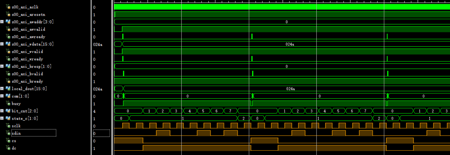
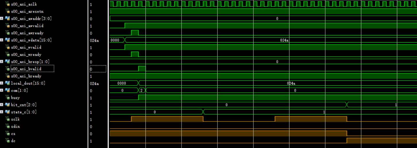
在CS为低时,串行输出为:0_1_0_0_1_0_1_0,正确完成SPI数据写功能。暂仅进行行为仿真,还没有上板验证,遇到问题后续改动更新。